信息检索报告范例
信息检索
综合检索报告
11 级 通信工程 专业
4 班
学 号 1 1 6 2 3 1 0 4 0 6
姓 名 史文倩
1、检索课题名称
LC谐振放大器(LC resonance amplifier)
2.检索策略
2.1 选择检索工具
中国期刊全文数据库(CNKI)
美国工程索引(EI)
中国专利信息中心
百度
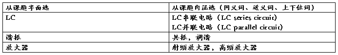
2.2选择检索词
3. 检索步骤及检索结果
3.1 中国期刊全文数据库(CNKI)
3.1.1 检索式
篇名=(LC串联+LC并联)*(谐振+调谐+共振)*(高频放大器+射频放大器)
3.1.2 检索年限 20##-2010
3.1.3检索结果
检索命中1452篇,选择5篇如下:
1、【篇名】基于单片机的自动调谐系统
【作 者】任红文,周庆国,许哲,石爱民,丛岩;
【出处】 微计算机信息20##年35期;
【摘要】本文介绍了利用单片机实现对高频发射机腔体自动调谐系统的控制,分析了系统的原理、结构及特点,重点探讨了系统所涉及的每个单元实现的功能及实现的方法。此系统用软件完成各信号的逻辑关系处理和输出,简化了硬件电路的设计,大大降低了系统的体积和开发成本。抗干扰设计从根本上保证了控制系统的稳定性和可靠性。
2、【篇名】射频功率放大器的优化设计
【作 者】李露;
【出处】 科教文汇(下旬刊)20##年09期
【摘要】本文提出了一种利用动态控制功率放大器的供应电源来达到提高射频功率放大器的效率的方法,它是利用频带不同宽度来动态调整功率放大器的供应电源。在较低输出功率时,可以减低功率放大器的供应电源,此方法可以节省硬件,在不牺牲输入信号的频宽的前提下,提高了功率放大器的使用效率。
3、【篇名】高效率中红外2.7μm可调谐激光器
【作 者】彭跃峰; 魏星斌; 王卫民; 李德明;
【出处】 光学学报20##年09期
【摘要】报道了采用1064nm激光抽运周期极化掺杂氧化镁的铌酸锂(PPMgO…CLN)晶体光参变振荡器(OPO)实现高效率2.7μm可调谐激光输出的实验结果,理论计算了PPMgO…CLN晶体准相位匹配(QPM)温度调谐曲线。在1064nm激光抽运功率为182W,声光Q开关工作频率为10kHz和PPMgO:CLN晶体工作温度为150℃条件下,获得了平均功率为36.7W、波长为2.73μm中红外激光输出,斜率效率为23.7%。通过改变周期为31.3μmPPMgO…CLN晶体的工作温度30℃~200℃,获得了中红外波长3.0~2.6μm激光输出,波长温度调谐实验结果与理论分析结果有大约10℃的差异。
4、【篇名】宽带射频功率放大器的匹配电路设计
【作 者】宫为保;
【出处】 广播电视信息20##年09期
【摘要】介绍了一种分析同轴线变换器的新方法,建立了理想与通用模型,降低了分析难度和简化了分析过程。通过研究分析,提出了一种同轴变换器与集总元件相结合的匹配电路设计方法,通过优化同轴线和集总元件的参数,实现放大器的最佳性能。利用该方法设计了一款应用于推挽式功率放大电路的匹配电路,仿真结果表明,匹配效率高达99.93%。
5、【篇名】基于负载牵引技术的射频功率放大器设计
【作 者】韦小刚; 吴明赞;
【出处】 电器电子教学学报20##年02期
【摘要】本文描述了微波电路中基于负载牵引技术的WLAN功率放大器的设计方法。笔者采用CMOS工艺设计了两级差分放大电路,并对该差分放大电路进行负载牵引。在此基础上,我们设计了输入输出匹配网络,最后使用ADS软件进行整体仿真。结果表明,在1.8V电源电压下,放大器增益为29dB,1dB压缩点的输出功率为18.3dBm,功率附加效率为16.8%,满足系统指标要求。
3.2 美国工程索引(EI)
3.2.1 检索式
(((((LC series circuit) WN KY) OR ((LC paralel circuit) WN KY)) AND ((resonance) WN KY)) AND ((amplifier) WN All fields))
3.2.2 检索年限 20##-2013
3.2.3 检索结果
命中25条结果,经过筛选,选择其中5条:
1、【篇名】A 900 MHz 26.8 dBm differential Class-E CMOS power amplifier
【作者】Wahab, Q.; Fritzin, J.; Alvandpour, A.; Wahab, Q.
【出处】German Microwave Conference, GeMIC 2010, March 15, 20## - March 17, 2010;
【摘要】A 900 MHz differential Class-E amplifier with finite dc inductance has been designed in CMOS. The large inductance of RF choke has been replaced with a finite inductance that provides the required inductive reactance of the class E amplifier. Resonance circuit is realized without series inductor by novel use of lattice LC balun. The amplifier delivers 26.8 dBm power to a 50 Ω load from a 2.2 V supply. A maximum Power Added Efficiency (PAE) of 43% is achieved.
2、【篇名】Low-harmonic push-pull class-E power amplifier with a pair of LC resonant networks
【作者】Chen, Feng-Yin Chen, Jiann-Fuh; Lin, Ray-Lee
【出处】IEEE Transactions on Circuits and Systems I: Regular Papers, v 54, n 3, p 579-589, March 2007;
【摘要】This paper proposes a novel push-pull Class-E series-parallel resonant power amplifier (PA), which parallels two basic one-inductor, one-capacitor Class-E high-efficiency switching-mode tuned PA (Sokal, 1981) circuits. This proposed topology utilizes a push-pull scheme to realize sinusoidal output voltage. The previously published Class-E circuits (Sokal, 1981) can be implemented in a very simplified circuit. However, the simplified circuit is only appropriate for applications in which the harmonic content of output is not an important criterion. The proposed amplifier with two series-parallel resonant load networks will allow sinusoidal output voltage to be achieved by associating with the positive and negative quasi-sinusoidal waveforms. The complementarily activated configuration will provide continuous high-ripple-frequency input-current waveforms; this approach significantly reduces electromagnetic interference and requires very little filtering. With the symmetry of the push-pull Class-E circuit, there is the additional benefit that the even harmonics are suppressed at the load, and thus there are fewer harmonic distortions. However, each switch is symmetrically driven with a duty ratio of less than 0.5 to meet the nominal Class-E operating conditions, which leads to a narrower operating frequency variation. A prototype of the proposed PA shows over 95% efficiency at 48-V input, with 18-W output and an operating frequency of 900 kHz.
3、【篇名】Linearity improvement of a power amplifier using a series LC resonant circuit
【作者】Kim, Ji HoonKim, Ki Young; Park, Chul Soon
【出处】IEEE Microwave and Wireless Components Letters, v 18, n 5, p 332-334, May 2008;
【摘要】A radio frequency power amplifier microwave monolithic integrated circuit with a series LC resonant circuit as well as a bias control circuit for wide-band code division multiple access application is presented. The linearizer that consists of a series LC resonant circuit and base-emitter junction of a bias transistor operates as a diode rectifier circuit. A comparison between the circuits with and without the linearizer has been demonstrated. The power amplifier (PA) with the series LC resonant linearizer exhibits adjacent channel leakage ratio-1 (ACLR1) of -37.2 dBc at output power of 27 dBm, a 5.6 dB improvement compared to the circuit without the linearizer. The bias control circuit reduces consumed average dc current from 83 mA to 57 mA for efficiency improvement. The linearized PA exhibits 1-dB compression point (P1dB) of 29.3 dBm, power-added efficiency of 45.7%, and power gain of 20.6 dB at low quiescent current of 37 mA with a 3.4 V single supply.
4、【篇名】Analysis and application of a parallel E-class amplifier as RF plasma source
【作者】Peña-Eguiluz, Rosendo; Pérez-Martínez, José Arturo; López-Callejas, Régulo; Mercado-Cabrera, Antonio; Solís-Pacheco, Josué; Aguilar-Uscanga, Blanca; Muñoz-Castro, Arturo E.; Valencia-Alvarado, Raúl; Barocio-Delgado, Samuel R.; Rodríguez-Méndez, Benjamín G.; De La Piedad-Beneitez, Aníbal
【出处】IEEE Transactions on Plasma Science, v 38, n 10 PART 2, p 2840-2847, October 2010;
【摘要】The design and construction of a 13.56-MHz RF power amplifier has been carried out on the basis of a modified resonant LC circuit in parallel regarding to the classic E-class amplifier LC series resonant circuit; this was done in order to take advantage of the operation characteristics of the resonant capacitor as a bidirectional voltage source. Therefore, the parallel LC circuit amplifies the voltage signals which can be applied to resistive or capacitiveresistive loads without the need for an impedance matching network, conventionally used with plasma generators. The main achievement of the described instrumentation lays in its constant response under a wide interval of load impedance. This facility has been applied to the generation of steady discharges in plasma needle appliances and both parallel plate and coaxial dielectric barrier discharge (DBD) reactors. Some relevant results of the DBD sterilization of four different kinds of microorganisms are included, showing the feasibility of the technique within reduced processing times, under 80 s in all the cases.
5、【篇名】A concurrent triple-band CMOS low noise amplifier for fourth generation applications
【作者】Jang, Yohan; Choi, Jaehoon
【出处】Microwave and Optical Technology Letters, v 53, n 2, p 415-418, February 2011;
【摘要】In this study, a concurrent triple-band low noise amplifier (LNA) is designed for long term evolution (LTE), Mobile-WiMAX (M-WiMAX), and WiMAX services. The main topology of the proposed LNA is a cascode architecture with source degeneration using shunt resistive feedback topology for the triple-resonance characteristic. The LNA is designed using a Taiwan Semiconduction Company (TSMC) 0.18 μm radio frequency CMOS process. To obtain the necessary gains over the operating frequency bands, a series LC branch is added in parallel with an inductor at the drain load of a single band LNA. The peak gains at LTE, M-WiMAX, and WiMAX bands are 17.6, 14.7, and 14.5 dB, respectively, whereas dissipating 8 mA from a 1.4 V supply voltage. The average noise figure over the three operating frequency bands is 4.5 dB. © 20## Wiley Periodicals, Inc. Microwave Opt Technol Lett 53:415-418, 2011; View this article online at wileyonlinelibrary.com. DOI 10.1002/mop.25743 Copyright © 20## Wiley Periodicals, Inc.
3.3 中国专利信息中心
3.3.1 检索式
F XX ((LC串联/TI+LC并联/TI)*(谐振/TI+调谐/TI+共振/TI)*(高频放大器/TI+射频放大器/TI))
3.3.2检索年限 20##-2013
3.3.3 检索结果
命中566条结果,经过筛选,选择其中5条:
1、【发明名称】利用了电容器-电抗器串联回路寄生参数的关联分析方法
【申请人】重庆市电力公司綦南供电局
【申请号】201110450575
【摘 要】本发明公开了一种利用了电容器-电抗器串联回路寄生参数的关联分析方法,包括以下步骤:步骤1:建立电力电容器、电抗器串联回路合-分闸操作过程技术分析等效电路模型;步骤2:将上述电路模型通过软件形式固化进硬件计算机中,形成关联分析系统;步骤3:将需要分析的相关参数输入关联分析系统,完成操作过电压的短路风险分析;本发明通过运用电路模型可以直接技术、分析、仿真出断路器机械运动过程与电过程中的电流电压分布规律,从而计算、分析出配电网电容器容量从1000~12000KVAR、串联电抗器从1~12%参数配置中的问题所在,并以此提出规避策略;为消除配网低规律因素回路操作事故提供了新的途径和方法,为提高电网的安全运行奠定可靠的基础。
2、【发明名称】一种半导体散热装置
【申请人】海洋王照明科技股份有限公司;深圳市海洋王照明技术有限公司
【申请号】201010502715
【摘 要】本发明适用于散热技术领域,提供了一种半导体散热装置。在本发明中,半导体散热装置与传统对发热电子元器件散热的风扇、散热片、热管等被动散热方式相比,利用具有热电能量转换特性的半导体材料,在通电时就具有制冷功能,主动迅速吸收发热电子元器件工作时产生的大量热量,同时,由于半导体散热装置的热端采用的陶瓷具有散热鳍片,加大了散热面积,因此散热效果更好,而且无噪音、无机械部件,使用更方便,从而使得电子元器件的工作效率更高,使用寿命更长。
3、【发明名称】LC调谐式静止无功发生器
【申请人】赵忠臣
【申请号】201110172452
【摘 要】本发明涉及一种LC调谐式静止无功发生器,属于无功补偿与调控技术领域。为了使电容器的容量连续平滑的变化和可调电抗器的输出波形不畸变,采用线性电抗器与电容器进行串、并联混合调谐的同时又组成了具有谐波治理能力的低通滤波器,对调控电流中的高次谐波旁路、扼制,实现了感性电流对容性谐振电流此大彼小、此小彼大的调控。无论是感性还是容性状态,输出电流都是连续平滑的变化,而且始终是正弦波。其只为容性状态时可以对系统进行可控的串、并联补偿;其在两种状态之间互相快速转变时可以成为动态无功补偿器(SVC)和静止调相器;还可以成为潮流控制器。
4、【发明名称】一种压降自动调整的串联回路取电电路
【申请人】上海工业自动化仪表研究院
【申请号】201010252657.9
【摘 要】本发明涉及一种压降自动调整的串联回路取电电路,包括依次串联的24V电源、串联型仪表设备、变送器、负载电阻,串联型仪表设备包括回路取电电路、DC/DC模块及内部电路,所述回路取电电路中串联一采样电阻,采样电阻上电压信号送入电压调整网络,电压调整网络驱动调节取电电路中串联在回路上晶体管的导通和截止,最终实现对回路压降的调节。电路实现简单,压降范围通过电路参数的选择可任意调整,并且适用于所有串联型回路取电仪表和设备,具有较广泛的推广应用价值。
5、【发明名称】振荡器内部动态信号源闭环仿真方法
【申请人】周世惕
【申请号】200910058535
【摘 要】本发明涉及一种振荡器内部动态信号源闭环仿真方法。该方法由仿真系统的结构、仿真步骤、仿真判据和仿真算法组成。任何电路的仿真都需要有信号源,而振荡器的仿真系统从原理上只允许有内部信号源,即内源,任何外源的介入都将破坏振荡器的条件。本发明从任一谐振元件中等效出电压型或者电流型内源,并赋予振荡器同时具有传输和负阻功能,从原理上解决了振荡器闭环仿真传输特性和负阻特性的难题。内源具有动态的内阻,对应的仿真采用了广义散射参数的算法。本发明提供了电路振荡的组合判据。在仿真实例中通过成功仿真高损耗晶体振荡器介绍了内源接入电路的不同方法。本仿真方法适用于不同器件、组态振荡器的仿真,并可用于新仿真软件的开发。
3.4 百度搜索引擎
3.4.1 检索式
title: ( "LC 谐振 放大器" );
3.4.2检索年限 20##-2013
3.4.3 检索结果
命中328条结果,经过筛选,选择其中5条:
1、【标题】LC放大器的进一步研究
【网址】http://www.cnki.com.cn/Article/CJFDTotal-LZKQ201106009.htm
【摘要】介绍了LC谐振放大器的设计方案与实现电路,主要由衰减器、谐振回路、放大器三个部分组成。衰减器采用纯电阻π型网络实现;谐振回路采用LC滤波电路设计;放大器采用功耗较小的2N2222A型三极管进行两级放大,输出结果时波形无明显失真。借助NI multisim仿真软件,对传统的设计进行了进一步的改进。
2、【标题】高增益LC谐振放大器的设计
【网址】http://www.cqvip.com/QK/90274X/201112/40743124.html
【摘要】采用分立元件设计了一个3级单调谐放大器,可用于通信接收机的前端电路,通过合理分配各级增益和多种措施提高抗干扰性,具有中心频率容易调整、稳定性高的特点。电路经实际测试表明具有低功耗、高增益和较好的选择性。
3、【标题】高频小信号LC谐振放大器的设计
【网址】http://www.cnki.com.cn/Article/CJFDTotal-KJIG201205032.htm
【摘要】本文介绍了高频小信号LC谐振放大器的设计思路与具体电路实现,主要由衰减网络、LC谐振放大、电压跟随和电源四大模块组成。衰减器采用电阻式π型网络实现;LC谐振放大中选用功耗小的2N2222型三极管进行两级放大,LC谐振部分为放大器的负载;电压跟随采用集成运放OPA355,以实现电路阻抗的良好匹配;为了给放大器工作提供稳压电源,采用LM317稳压芯片设计了一个电源。经测试,放大器低功耗、高增益,具有良好的选择性。
4、【标题】高增益LC谐振放大器的设计
【网址】http://www.eefocus.com/analog-power/317563
【摘要】采用分立元件设计了一个3级单调谐放大器,可用于通信接收机的前端电路,通过合理分配各级增益和多种措施提高抗干扰性,具有中心频率容易调整、稳定性高的特点。电路经实际测试表明具有低功耗、高增益和较好的选择性。
5、【标题】高增益LC谐振放大器的设计
【网址】http://d.wanfangdata.com.cn/Periodical_dzjs201112025.aspx
【摘要】采用分立元件设计了一个3级单调谐放大器,可用于通信接收机的前端电路,通过合理分配各级增益和多种措施提高抗干扰性,具有中心频率容易调整、稳定性高的特点.电路经实际测试表明具有低功耗、高增益和较好的选择性。
3.综述
引言
-
文献检索报告(例文)
浅谈茶文化对经济的影响以贵州湄潭为例文献信息检索报告学院六盘水师范学院姓名学号专业20xx年6月9日六盘水师范学院20xx年春季学…
-
文献信息检索报告范文
信息检索报告学院专业学号姓名课题名称基于单片机的电能表电路的研究课题名称英文Accordingtothesearchofelect…
-
信息检索报告实例
检索报告题目后现代主义对教育的影响姓名学号系别计科系专业网络技术20xx年12月6日检索报告一课题分析1课题名称后现代主义对教育的…
-
信息检索报告范文
一我选择的检索课题是为考英语四级考试搜集信息二和这个课题相关的信息需求主要有a英语四级考试日期b英语四级考试报名c考生考试应注意的…
-
信息检索报告范例
信息检索综合检索报告专业:通信工程学号:XX姓名:XX1、检索课题名称LC谐振放大器(LCresonanceamplifier)2…
-
文献检索报告范文
文献检索报告20**级临床7班1.检索题目:甲巯咪唑治疗甲亢的不良反应2.检索过程:(1)课题分析:甲状腺功能亢进症简称甲亢,是由…
-
文献检索报告范文
科技信息检索检索报告级专业班学号姓名说明利用所学的文献信息检索知识和检索方法,结合自己的专业,自定检索课题,从多方面广泛收集有关资…
-
信息检索 报告 和学习报告范文
服装学院20xx级服装设计专业姓名陈柯竹学号20xx531201联系电话183xxxxxxxx本科课程考查专用封面作业题目信息检索…
-
文献信息检索报告范文
信息检索报告课程名称空调的节电控制装置学院专业学号姓名完成时间20xx年03月22日课题名称空调的节电控制装置课题名称英文Elec…
-
文献检索报告范文
信息检索检索报告级专业班学号姓名说明利用所学的文献信息检索知识和检索方法结合自己的专业自定检索课题从多方面广泛收集有关资料并完成该…
-
信息检索学习总结报告
一、自我评价对于本学期的信息检索课程,我自认为自己认真积极,从不缺课、迟到、早退,学习尽心尽力。对于老师讲解的知识也掌握的较为清楚…