毕业设计(论文)基本要求(附录)
附录A.1 北京石油化工学院
本科生毕业设计(论文)撰写格式(试行)
为保证我校本科生毕业设计(论文)质量,培养学生严谨的科学作风,特制定本撰写格式。本格式适用于我校所有本科生专业毕业论文的撰写。
一、 撰写格式
1.中文摘要、英文摘要、目录、正文的各章、参考文献、致谢、附录均另起一页,论文的题目、学生姓名、指导教师姓名等信息只需在毕业论文的封面及封二提供,其他地方无须填写。
封面、封二和任务书上的内容用钢笔填写或打印,必须正确无误。论文题目控制在20个汉字以内。
2.论文的章、节编号
论文的大标题为第一章、第二章……,“第一章”后空两格不加标点,然后写大标题的内容,大标题居中。
正文中使用的一级节标题为:1.1、1.2……,2.1、2.2……,一级节标题均另起一行居左;二级节标题为1.1.1、1.1.2……,另起一行空两格写二级节标题。节标题题序数目字后空一格,不加标点。
3.论文字体、字型及字号要求及其举例
内容 举例 中文字号 英文字号
大标题 第一章 黑体三号 Times New Roman 三号
(中英文“摘要”、“参考文献”、“致谢”、“附录”与大标题格式同)
一级节标题 4.1实验方法 黑体四号 Times New Roman 四号
二级节标题 3.2.2 实验装置 黑体小四号 Times New Roman 小四号
正 文 实验取得预期效果 宋体小四 Times New Roman 小四
表题与图题 图3.8 pH化学破碎的影响 宋体五号 Times New Roman 五号
参考文献及页眉 无机化工工艺学 宋体五号 Times New Roman 五号
目录中的大标题 第一章 黑体小四号 Times New Roman 小四
目录中的一级节标题 2.1 概述 宋体小四号 Times New Roman 小四
目录中二级节标题 2.1.1 宋体五号字 Times New Roman 五号
4.段落及行间距要求
·正文段落和各级标题(包含中英文摘要、目录、致谢)一律取“固定行间距21磅”,正文段落首行缩进两个中文字符;正文中公式所在行的行距设为“单倍行距”。
·按照标题级别不同,分别采用不同的段前、后间距:
标题级别 段前间距 段后间距
大标题 12磅 18 磅
一级节标题 12磅 12 磅
二级节标题 6磅 6 磅
(可适当调节各级标题的段前、后间距,以利于控制正文合适的换页位置)
·目录正文中的段落间距为21~25磅(可根据实际情况做适当调整)。
·参考文献,标题的段前间距为12磅,段后间距为18磅。参考文献正文取固定行距21磅,注意不要在一篇参考文献段落的中间换页。
·附录部分,标题的行间距21磅,段前、段后间距分别为12磅、18磅,正文部分采用小四号字体,行间距为18磅。
5.摘要
中英文摘要格式见范文,摘要的关键词在摘要正文后空一行,排在摘要的左下方。关键词之间用逗号隔开,最后一词不加标点符号。
6.页眉与页码
将论文的题目作为页眉(附录和声明部分的页眉不作要求),采用五号宋体,居中。
论文页码一律用阿拉伯数字(五号字、Times New Roman、居中)连续编码,页码由第1章的首页开始作为第1页。论文前置部分(摘要、目录)的页码须采用罗马数字(Ⅰ、Ⅱ、……)单独编号。
7.图、表和公式等
图、表、公式等与正文之间要有一行的间距。
·图:要精选,要具有自明性,切忌与表和文字表述重复;要清楚,但坐标比例不要过分放大,同一图上不同曲线的点要分别用不同形状的标示符标出;图中的术语、符号、单位等应与文字表述中所用的一致;图中的文字使用五号宋体。图的序号和图名居中置于图的下方,段前间距为6磅,段后间距为0。
·表:采用三线式表格,上下两根线宽设置为3/2磅,中间一根线宽为1/2磅。根据具体情况,在三线式表格中可适当增加辅助线,以适应较复杂表格的需要。表中参数应标明量和单位表示符号;表格允许下页接写,接写时表题省略,表头应重复书写,即在表右上方写“续表××”。表中的数字、文字均用五号宋体或更小字体。表的序号和表名居中置于表的上方,段前间距为0,段后间距为6磅。
·公式:用公式编辑器编辑,公式较长时最好在等号“=”处转行, 如难实现,则可在+、-、×、÷运算符号处转行,转行时运算符号仅书写于转行式前,不重复书写。
文中的图、表、附注、公式一律采用阿拉伯数字分章编号。如:图2-5;表3-2;公式(5-1)等。若图或表中有附注,其对应采用英文小写字母顺序编号;附注写在图或表的下方。
8.参考文献
参考文献为正式或非正式出版的刊物(包括印刷版和电子版)或学位论文、研究报告、学会论文集等文献资料。参考文献表采用引用顺序编码制组织。建议根据《中国高校自然科学学报编排规范》的要求书写参考文献,并按顺序编码制,即按引用的顺序将参考文献附于文末,正文中引用部分按出现的先后顺序编号,将文献序号作为右上角标,置于方括号内(引用多篇文献时,只须将各篇文献的序号在方括号内全部列出,各序号间用“,”,如李伟[57, 83]提出……;如遇连续序号,可标注起迄序号,如莫拉德对稳定区的机理研究[57~60])。作者姓名写到第三位,余者写“,等”或“,et al.”,多个作者之间以“,”区分。
几种主要参考文献著录表的格式为:
期 刊 论 文:[序号]作者. 文题[J]. 刊名,出版年,卷号(期号):起~止页码
专(译)著: [序号]作者. 书名[M](译者).版本. 出版地:出版者,出版年. 起~止页码
论 文 集:[序号]作者. 文题[C]:编者,编. 论文集名.出版地:出版者,出版年. 起~止页码
学 位 论 文:[序号]作者. 文题[D]:[XX学位论文]. 授予单位所在地:授予单位,授予年
专利文献:[序号]申请者. 专利名[P]. 国名,专利文献种类,专利号,出版日期
技术标准:[序号]发布单位. 技术标准代号. 技术标准名称[S]. 出版地:出版者,出版日期
报 纸:[序号] 作者. 文题[N]. 报纸名. 出版日期(版次)
技术报告:[序号] 作者. 文题[R]. 保存地点:年份
电子文献:[序号] 作者. 文题[电子文献及载体类型标识]. 文献出处. 日期
几种文献类型及其标识为:
期刊[J] 专著[M] 论文集[C] 学位论文[D]
专利[P] 标准[S] 报纸[N] 技术报告[R]
几种电子文献载体及其标识为:
磁带[MT] 磁盘[DK] 光盘[CD] 联机网络[OL]
网上数据库[DB/OL] 光盘图书[M/CD]
磁带数据库[DB/MT] 磁盘软件[CP/DK]
网上期刊[J/OL] 网上电子公告[EB/OL]
9.附录
格式见范文。论文的附录顺次为附录l,附录2…编号。附录中的图和公式另编排序号,与正文分开。
10.名词、名称
科学技术名词术语应采用全国自然科学名词审定委员会公布的规范词或国家标准、部标准中规定的名称,尚未统一规定或叫法有争议的名称术语,可采用惯用的名称;使用外文缩写代替某一名词术语时,首次出现时应在括号内注明其含义,外国人名一般采用英文原名,一般很熟知的外国人名(如牛顿、达尔文、马克思等)可按通常标准译法写译名。
11.标点符号
论文中的标点符号按新闻出版署公布的“标点符号用法”使用。
12. 量和单位
论文采用1984年2月27日国务院发布的《中华人民共和国法定计量单位》,并遵照《中华人民共和国法定计量单位使用方法》执行。单位名称和符号的书写方式一律采用国际通用符号。
二、 打印及装订要求
1.论文一律用计算机排版打印,建议使用WORD97以上版本。论文纸张用A4标准白纸(210mm-297mm),单面打印。
2.论文页面设置:版面页边距上空3.5cm、下3.5cm、左空3.2cm、右空2.7cm,装订线0cm、位置左侧,页眉2.5cm、页脚2.5cm,正文采用固定行间距为21磅,标准字符间距。
3.论文的页眉填写设计(论文)的题目,中文摘要、外文摘要和目录的页码用罗马数字编号,从正文开始用阿拉伯数字编码。
4.设计(论文)用教务处统一封面、按顺序:1.封面(及封二);2.任务书;3.中文摘要(含关键词);4.外文摘要(含关键词);5.目录;6.正文;7.参考文献;8.致谢;9.附录;10.声明;11.封底,装订成册。
附录A.2
北京石油化工学院
本科毕业设计(论文)开题报告
题目名称:
题目类型:
学生姓名:
专 业:
学 院:
年 级:
指导教师:
年 月 日
一、 选题背景、研究意义及文献综述
1、 选题背景
2、 研究意义
3、 文献综述
二、 研究的基本内容,拟解决的主要问题
三、 研究步骤、方法
四、 研究工作进度
五、 主要参考文献
六、 系(教研室)评议意见
评议人:
年 月 日
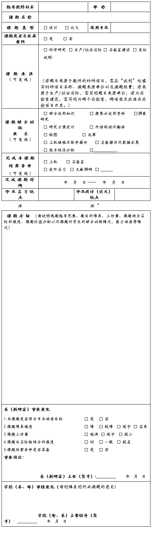
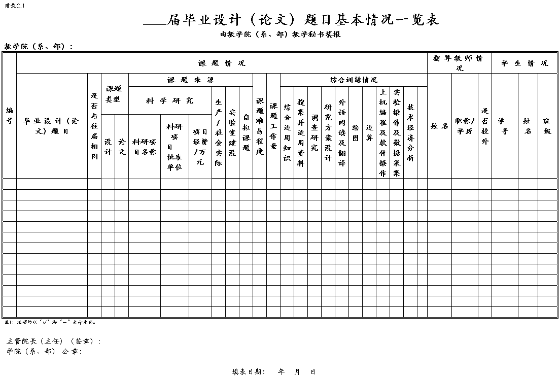
附录B.1
毕业设计(论文)题目申报表(参考使用)
( - 学年)
教学院(系、部):
附录B.2
北 京 石 油 化 工 学 院
毕 业 设 计 (论 文) 任 务 书
教学院(系、部) 专业 班级
学生姓名 指导教师/职称
1.毕业设计(论文)题目
2.任务起止日期: 年 月 日 至 年 月 日
3.毕业设计(论文)的主要内容与要求
(含课题简介、任务与要求、预期培养目标、原始数据及应提交的成果)

4.主要参考文献
5.进度计划及指导安排
任务书审定日期 年 月 日 系(教研室)主任(签字)
任务书批准日期 年 月 日 教学院(系、部)院长(签字)
任务书下达日期 年 月 日 指导教师(签字)
计划完成任务日期 年 月 日 学生(签字)
附录D.1 北 京 石 油 化 工 学 院
毕业设计(论文)指导教师评语
学生姓名 班级 指导教师/职称
毕业设计(论文)题目

北 京 石 油 化 工 学 院
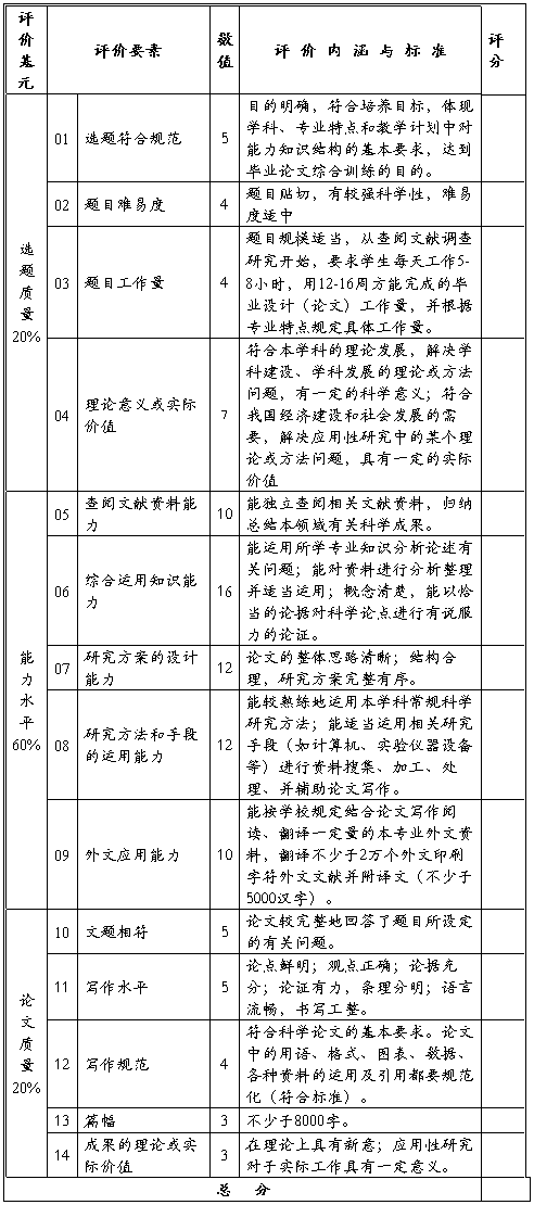
毕业设计(论文)指导教师评分标准及评分表(参考使用)
(理工类)
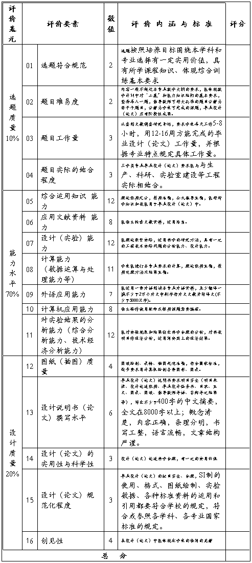
注:供各专业参考使用,需包含“选题质量、能力水平和设计质量”三项评价基元,评价基元各项所占比例及“评价要素”、“数值”等内容可自行制定。
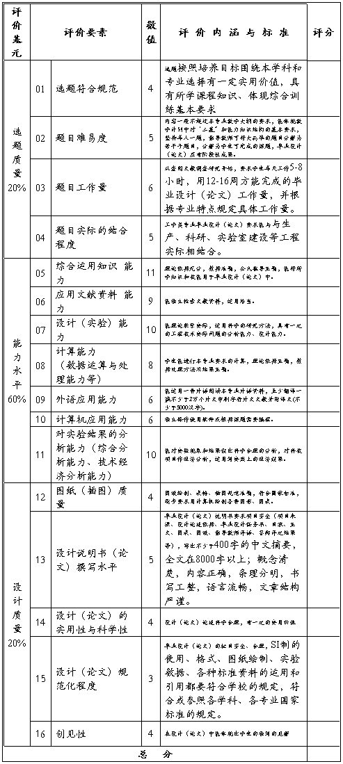
北 京 石 油 化 工 学 院
毕业设计(论文)指导教师评分标准及评分表(参考使用)
(文管类)

注:供各专业参考使用,需包含“选题质量、能力水平和设计质量”三项评价基元,评价基元各项所占比例及“评价要素”、“数值”等内容可自行制定。
附录D.2 北 京 石 油 化 工 学 院
毕业设计(论文)评阅教师评语
学生姓名 班级

北 京 石 油 化 工 学 院
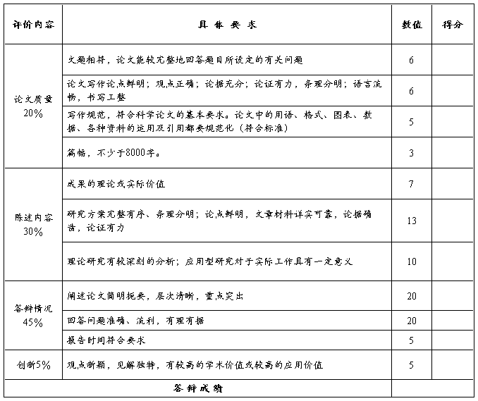
毕业设计(论文)评阅教师评分标准及评分表(参考使用)
(理工类)
注:供各专业参考使用,需包含“选题质量、能力水平和设计质量”三项评价基元,评价基元各项所占比例及“评价要素”、“数值”等内容可自行制定。
北 京 石 油 化 工 学 院
毕业设计(论文)评阅教师评分标准及评分表(参考使用)
(文管类)
注:供各专业参考使用,需包含“选题质量、能力水平和设计质量”三项评价基元,评价基元各项所占比例及“评价要素”、“数值”等内容可自行制定。
附录D.3 北 京 石 油 化 工 学 院
毕业设计(论文)答辩小组评语
学生姓名 班级

北 京 石 油 化 工 学 院
毕业设计(论文)答辩小组评分标准及评分表(参考使用)
(理工类)
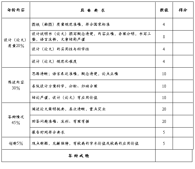
注:供各专业参考使用,需包含“设计(论文)质量、陈述内容和答辩情况”三项评价内容,评价内容各项所占比例及“具体要求”、“数值”等内容可自行制定。
北 京 石 油 化 工 学 院
毕业设计(论文)答辩小组评分标准及评分表(参考使用)
(文管类)
注:供各专业参考使用,需包含“论文质量、陈述内容和答辩情况”三项评价内容,评价内容各项所占比例及“具体要求”、“数值”等内容可自行制定。
附录D.4
北 京 石 油 化 工 学 院
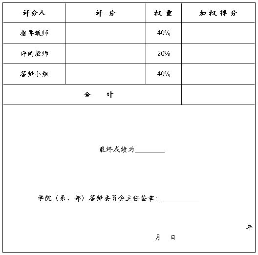
毕业设计(论文)成绩单
学院(系、部) 专业 班级
学生姓名 指导教师/职称
毕业设计(论文)题目
附录D.5 北 京 石 油 化 工 学 院
毕业设计(论文)答辩记录
学生姓名 班级
答辩时间: 年 月 日 ~ 时
答辩地点:

第二篇:毕业设计(论文)附录
北京信息科技大学
毕业设计(论文)附录
题目:基于单片机的数字钟的设计
学院:自动化学院
专业:自动化
学生姓名:崔智明 班级/学号:06331/16
指导老师/督导老师:唐胜春/
起止时间:20xx年 3月 21日至20xx年 6月 10日
目录
附件1:基于单片机的英语论文及翻译…………………………………共 9页 附件2:软件程序…………………………………………………………共 18页
基于单片机的英语论文及翻译
Programmable controllers
From a simple heritage, these remarkable systems have evolved to not only replace electromechanical devices, but to solve an ever-increasing array of control problems in both process and nonprocess industries. By all indications, these microprocessor
powered giants will continue to break new ground in the automated factory into the 1990s. HISTORY
In the 1960s, electromechanical devices were the order of the day ass far as control was concerned. These devices, commonly known as relays, were being used by the thousands to control many sequential-type manufacturing processes and stand-along machines. Many of these relays were in use in the transportation industry, more specifically, the automotive industry. These relays used hundreds of wires and their interconnections to effect a control solution. The performance of a relay was basically reliable - at least as a single device. But the common applications for relay panels called for 300 to 500 or more relays, and the reliability and maintenance issues associated with supporting these panels became a very great challenge. Cost became another issue, for in spite of the low cost of the relay itself, the installed cost of the panel could be quite high. The total cost including purchased parts, wiring, and installation labor, could range from $30~$50 per relay. To make matters worse, the constantly changing needs of a process called for recurring modifications of a control panel. With relays, this was a costly prospect, as it was accomplished by a major rewiring effort on the panel. In addition these changes were sometimes poorly documented, causing a second-shift maintenance nightmare months later. In light of this, it was not uncommon to discard an entire control panel in favor of a new one with the appropriate components wired in a manner suited for the new process. Add to this the unpredictable, and potentially high, cost of maintaining these systems as on high-volume motor vehicle production lines, and it became clear that something was needed to improve the control process – to make it more reliable, easier to troubleshoot, and more adaptable to changing control needs.
That something, in the late 1960s, was the first programmable controller. This first ‘revolutionary’ system wan developed as a specific response to the needs of the major automotive manufacturers in the United States. These early controllers, or programmable logic controllers (PLC), represented the first systems that 1 could be used on the factory floor, 2 could have there ‘logic’ changed without extensive rewiring or component changes, and 3 were easy to diagnose and repair when problems occurred.
It is interesting to observe the progress that has been made in the past 15 years in the programmable controller area. The pioneer products of the late 1960s must have been confusing and frightening to a great number of people. For example, what happened to the hardwired and electromechanical devices that maintenance personnel were used to repairing with hand tools? They were replaced with ‘computers’ disguised as electronics designed to replace relays. Even the programming tools were designed to appear as relay
equivalent presentations. We have the opportunity now to examine the promise, in retrospect, that the programmable controller brought to manufacturing.
All programmable controllers consist of the basic functional blocks shown in Fig. 10. 1. We’ll examine each block to understand the relationship to the control system. First we look at the center, as it is the heart ( or at least the brain ) of the system. It consists of a microprocessor, logic memory for the storage of the actual control logic, storage or
variable memory for use with data that will ordinarily change as a function power for the processor and memory. Next comes the I/O block. This function takes the control level signals for the CPU and converts them to voltage and current levels suitable for
connection with factory grade sensors and actuators. The I/O type can range from digital (discrete or on / off), analog (continuously variable), or a variety of special purpose ‘smart’ I/O which are dedicated to a certain application task. The programmer is shown here, but it is normally used only to initially configure and program a system and is not required for the system to operate. It is also used in troubleshooting a system, and can prove to be a valuable tool in pinpointing the exact cause of a problem. The field devices shown here represent the various sensors and actuators connected to the I/O. These are the arms, legs, eyes, and ears of the system, including push buttons, limit switches, proximity switches, photosensors, thermocouples, RTDS, position sensing devices, and bar code reader as input; and pilot lights, display devices, motor starters, DC and AC drives, solenoids, and printers as outputs.
No single attempt could cover its rapidly changing scope, but three basic
characteristics can be examined to give classify an industrial control device as a programmable controller.
(1) Its basic internal operation is to solve logic from the beginning of memory to some specified point, such as end of memory or end of program. Once the end is reached, the operation begins again at the beginning of memory. This scanning process continues from the time power is supplied to the time it it removed.
(2) The programming logic is a form of a relay ladder diagram. Normally open,
normally closed contacts, and relay coils are used within a format utilizing a left and a right vertical rail. Power flow (symbolic positive electron flow) is used to determine which coil or outputs are energized or deenergized.
(3) The machine is designed for the industrial environment from its basic concept; this protection is not added at a later date. The industrial environment includes unreliable AC power, high temperatures (0 to 60 degree Celsius), extremes of humidity, vibrations, RF noise, and other similar parameters.
General application areas
The programmable controller is used in a wide variety of control applications today, many of which were not economically possible just a few years ago. This is true for two general reasons: 1 there cost effectiveness (that is, the cost per I/O point) has improved dramatically with the falling prices of microprocessors and related components, and 2 the ability of the controller to solve complex computation and communication tasks has made it possible to use it where a dedicated computer was previously used.
Applications for programmable controllers can be categorized in a number of different ways, including general and industrial application categories. But it is important to
understand the framework in which controllers are presently understood and used so that the full scope of present and future evolution can be examined. It is through the power of applications that controllers can be seen in their full light. Industrial applications include many in both discrete manufacturing and process industries. Automotive industry
applications, the genesis of the programmable controller, continue to provide the largest base of opportunity. Other industries, such as food processing and utilities, provide current development opportunities.
There are five general application areas in which programmable controllers are used.
A typical installation will use one or more of these integrated to the control system problem. The five general areas are explained briefly below.
Description:
The AT89C51 is a low-power, high-performance CMOS 8-bit microcomputer with 4K bytes of Flash programmable and erasable read only memory (PEROM). The device is manufactured using Atmel’s high-density nonvolatile memory technology and is
compatible with the industry-standard MCS-51 instruction set and pinout. The on-chip Flash allows the program memory to be reprogrammed in-system or by a conventional nonvolatile memory programmer. By combining a versatile 8-bit CPU with Flash on a monolithic chip, the Atmel AT89C51 is a powerful microcomputer which provides a highly-flexible and cost-effective solution to many embedded control applications. Function characteristic
The AT89C51 provides the following standard features: 4K bytes of Flash, 128 bytes of RAM, 32 I/O lines, two 16-bit timer/counters, a five vector two-level interrupt
architecture, a full duplex serial port, on-chip oscillator and clock circuitry. In addition, the AT89C51 is designed with static logic for operation down to zero frequency and supports two software selectable power saving modes. The Idle Mode stops the CPU while
allowing the RAM, timer/counters, serial port and interrupt system to continue functioning. The Power-down Mode saves the RAM contents but freezes the oscillator disabling all other chip functions until the next hardware reset.
Pin Description
VCC:Supply voltage.
GND:Ground.
Port 0:
Port 0 is an 8-bit open-drain bi-directional I/O port. As an output port, each pin can sink eight TTL inputs. When 1s are written to port 0 pins, the pins can be used as
highimpedance inputs.Port 0 may also be configured to be the multiplexed loworder
address/data bus during accesses to external program and data memory. In this mode P0 has internal pullups.Port 0 also receives the code bytes during Flash programming,and outputs the code bytes during programverification. External pullups are required during programverification.
Port 1
Port 1 is an 8-bit bi-directional I/O port with internal pullups.The Port 1 output buffers can sink/source four TTL inputs.When 1s are written to Port 1 pins they are pulled high by the internal pullups and can be used as inputs. As inputs,Port 1 pins that are externally being pulled low will source current (IIL) because of the internal pullups.Port 1 also receives the low-order address bytes during Flash programming and verification. Port 2
Port 2 is an 8-bit bi-directional I/O port with internal pullups.The Port 2 output buffers can sink/source four TTL inputs.When 1s are written to Port 2 pins they are pulled high by the internal pullups and can be used as inputs. As inputs,Port 2 pins that are externally being pulled low will source current, because of the internal pullups.Port 2 emits the high-order address byte during fetches from external program memory and during
accesses to external data memory that use 16-bit addresses. In this application, it uses strong internal pullupswhen emitting 1s. During accesses to external data memory that use 8-bit addresses, Port 2 emits the contents of the P2 Special Function Register.Port 2 also receives the high-order address bits and some control signals during Flash
programming and verification.
Port 3
Port 3 is an 8-bit bi-directional I/O port with internal pullups.The Port 3 output buffers can sink/source four TTL inputs.When 1s are written to Port 3 pins they are pulled high by the internal pullups and can be used as inputs. As inputs,Port 3 pins that are externally being pulled low will source current (IIL) because of the pullups.Port 3 also serves the functions of various special features of the AT89C51 as listed below:
Port 3 also receives some control signals for Flash programming and verification. RST
Reset input. A high on this pin for two machine cycles while the oscillator is running resets the device.
ALE/PROG
Address Latch Enable output pulse for latching the low byte of the address during accesses to external memory. This pin is also the program pulse input (PROG) during Flash programming.In normal operation ALE is emitted at a constant rate of 1/6 the oscillator frequency, and may be used for external timing or clocking purposes. Note, however, that one ALE pulse is skipped during each access to external Data Memory. If desired, ALE operation can be disabled by setting bit 0 of SFR location 8EH. With the bit set, ALE is active only during a MOVX or MOVC instruction. Otherwise, the pin is weakly pulled high. Setting the ALE-disable bit has no effect if the microcontroller is in external execution mode.
PSEN
Program Store Enable is the read strobe to external program memory.When the AT89C51 is executing code from external program memory, PSEN is activated twice each machine cycle, except that two PSEN activations are skipped during each access to external data memory.
EA/VPP
External Access Enable. EA must be strapped to GND in order to enable the device to fetch code from external program memory locations starting at 0000H up to FFFFH. Note, however, that if lock bit 1 is programmed, EA will be internally latched on reset.EA should be strapped to VCC for internal program executions.This pin also receives the 12-volt programming enable voltage(VPP) during Flash programming, for parts that
require12-volt VPP.
XTAL1
Input to the inverting oscillator amplifier and input to the internal clock operating circuit. XTAL2
Output from the inverting oscillator amplifier.
Oscillator Characteristics
XTAL1 and XTAL2 are the input and output, respectively,of an inverting amplifier which can be configured for use as an on-chip oscillator, as shown in Figure 1.Either a quartz crystal or ceramic resonator may be used. To drive the device from an external clock source, XTAL2 should be left unconnected while XTAL1 is driven as shown in Figure
2.There are no requirements on the duty cycle of the external clock signal, since the input to the internal clocking circuitry is through a divide-by-two flip-flop, but minimum and maximum voltage high and low time specifications must be observed.
Figure 1. Oscillator Connections Figure 2. External Clock Drive Configuration Idle Mode
In idle mode, the CPU puts itself to sleep while all the onchip peripherals remain active. The mode is invoked by software. The content of the on-chip RAM and all the special functions registers remain unchanged during this mode. The idle mode can be terminated by any enabled interrupt or by a hardware reset.It should be noted that when idle is terminated by a hard ware reset, the device normally resumes program execution,from where it left off, up to two machine cycles before the internal reset algorithm takes control. On-chip hardware inhibits access to internal RAM in this event, but access to the port pins is not inhibited. To eliminate the possibility of an unexpected write to a port pin when Idle is terminated by reset, the instruction following the one that invokes Idle should not be one that writes to a port pin or to external memory.
Power-down Mode
In the power-down mode, the oscillator is stopped, and the instruction that invokes power-down is the last instruction executed. The on-chip RAM and Special Function
Registers retain their values until the power-down mode is terminated. The only exit from power-down is a hardware reset. Reset redefines the SFRs but does not change the on-chip RAM. The reset should not be activated before VCC is restored to its normal operating level and must be held active long enough to allow the oscillator to restart and stabilize.
Program Memory Lock Bits
On the chip are three lock bits which can be left unprogrammed (U) or can be
programmed (P) to obtain the additional features listed in the table below.
When lock bit 1 is programmed, the logic level at the EA pin is sampled and latched during reset. If the device is powered up without a reset, the latch initializes to a random value, and holds that value until reset is activated. It is necessary that the latched value of EA be in agreement with the current logic level at that pin in order for the device to function properly
可编程控制器
从一个简单的遗产,到这些卓越的系统,已经发展到不仅取代机电设备,而是要解决一个过程,机电行业历来都增加数组的控制问题。 所有迹象表明,在上世纪90年代投入自动化工厂,这些微处理器巨头将继续打破新的局面。
历史 :
在20世纪60年代,就控制而言,机电设备是家常便饭。 这些设备,通常称为继电器,如正在使用的数以千计的控制多序列型制造工艺和独立式机器。继电器许多人在使用,特别在运输行业,更是汽车行业。 这些继电器用于数百电线及其相互联系,以实施控制解决方案。 继电器性能基本上是一个可靠的-至少作为一个单一的设备。 但控制板上有300至500名或以上继电器,这些面板的可靠性和相关的维修问题成为一个很大的挑战。 成本成为另一个问题,尽管面板在成本低的安装成本继电器本身,可能相当高。 总成本包括购买零件,布线,安装和劳动力,大概是每个30元?50元。 更糟的是,一个控制面板的不断反复修改的过程称为一个不断变化的需求。 与继电器相比,这是一个昂贵的过程,因为它是由小组完成的一项重大工作,重新布线。 此外,这些变化有时成果不佳,导致个月后的第二次移维修的恶梦。从这一点出发的,这并非罕见地放弃了一个适用于整个有线控制面板,而是在适当时候的有利的新进程。 除此之外,还有不可预测的,潜在的高成本生产线,汽车的成本维护这些系统,高容量,它显然需要一些改进控制程序,使之更可靠,更容易解决问题,并更能适应不断变化的控制需求。
在20世纪60年代末,第一个可编程序控制器产生了。 这第一'革命'系统发展成为一个对美国制造商的需要具体的回应,主要应用在汽车上。 这些早期的控制器,或可编程逻辑控制器(PLC),生产和修复系统,首先用于工厂车间,它还可有'或逻辑可以使'没有广泛改变重新布线组成部分发生变化,也可以例诊断时容易发生的问题。
有趣的是,观察该产品的进展,取得了控制器的可编程过去15年的成果。 20世纪60年代末的先驱产品,是可怕的,混乱的,需要大量的人力。 例如,发生了什么的硬件连线和机电工具设备问题,维修人员用手工来修复?不, 他们改为'电脑'继电器装成电子设计来取代。 即使是编程工具的设计,均显示为电脑继电,相当于演示。 现在我们有机会看看当时的承诺,在今日看来,当时的可编程控制器带来了生产革新。
我们来看看所有可编程控制器组成的基本功能。 我们将检查每块了解关系到控制系统。 首先,我们看看它的中心,因为它是心脏(或至少是大脑系统)的。 它包括一个微处理器,控制逻辑的实际内存的存储器,储存或可变存储器和使用的数据通常会改变处理器的运行结果。 其次是在I / O块。 此模块为CPU控制电平信号,并将其转换与工厂的连接传感器和驱动器它们的电压和电流合适的水平。 该I / O块的范围从数字(离散或开/关),模拟(连续变量),或者是'各种特殊用途的'的,I / O是专用于某些应用程序的任务的模块。 在程序员的这里显示是最初设定的制度和程序,是不能运作所的系统。 它也可以用来排除故
障的工具,已被证明是一个有价值的工具,可以找出针对问题的确切原因。 现场设备显示在这里好像各种传感器和执行器连接到产品的 胳膊,腿,眼,耳和系统的,如按钮,限位开关,接近开关,photosensors,热电偶,RTD,位置传感设备,条码技术被用作输入码阅读器和指示灯,显示设备,电机起动器,直流和交流驱动器,电磁阀,如打印机和产出。 没有任何单一的检测可概括的迅速变化,但三个基本特征可以进行检查,以给归类为一个可编程控制器的工业控制装置。
(1)它的基本的内部运作是从一开始就一些具体问题解决内存逻辑,如程序存储器或年底结束。 一旦达到目的,操作重新开始在存储的开端。 该扫描过程持续时间是从删除它到间接通电源。
(2)编程逻辑图表形式继电器阶梯。 常开,常闭触点,继电器线圈和一个左内使用的格式,并正确利用一个垂直的轨道。 潮流(符号正电子流)用来确定哪些线圈通电或输出或deenergized。
(3)本机是专为工业环境设计的,这种保护是没有日期在稍后加入。 工业环境包括不可靠的交流电源,高温度(0至60摄氏度),湿度极端的,振动,射频噪音,以及其他类似的特殊环境。
一般应用领域 :
可编程控制器是用于多种应用控制的今天,其中许多是几年前不可能想象的解决办法。 真正的原因有两个:一有成本效益(即每点成本的I / O),它已经通过相关组件的价格下跌的微处理器得到了很大的改善,二控制器的能力,它可解决复杂的计算和通信任务,使人们有可能用它好像是使用的一台以前的专用计算机。
可编程控制器的应用可按不同方式分为若干类别,包括普通和工业应用。 但重要的是要了解所使用的框架,就目前的理解,控制器在未来应该可以全面审查问题。可以看到它通过线路通过传输指令,达到控制器的应用程序使用。 工业应用包括很多行业,主要是在离散制造和流程。 汽车行业的应用是可编程控制器的成因,是可编程控制器继续做大的基地。 其他行业,如食品加工和工具也提供了发展机遇。
可编程控制器有一般应用在哪5个领域。 一个典型的安装将使用一个或多个这些集成到控制系统的问题。 这五个一般领域下文将简要解释。
描述:
该基于AT89C51是一种低功耗,高性能和可擦除可编程闪存的CMOS 8位单片机具有4K字节的只读存储器(派罗姆)。 该设备是采用Atmel的高密度非易失性内存技术,是引脚兼容业界标准的MCS - 51指令集和。 片上闪存程序存储器可以被重新编程在系统或传统的非易失性内存程序员。 通过结合位CPU芯片上的闪存的单片多功能8位时钟,爱特梅尔AT89C51的是一个强大的微型控制器提供了一个高度灵活和成本效益的解决方案,许多嵌入式控制应用。
功能特点:
该单片机AT89C51提供以下标准功能:4K的芯片字节的闪存,128字节的RAM,32个 I / O,两个16位定时器/计数器,1 5向量2级中断结构,一个全双工串行口,振荡器和时钟电路。 此外,AT89C51的设计与零频率静态逻辑的运作,并支持两种软件可选的节电模式。 空闲模式下停止CPU的工作,而RAM,定时/计数器,串口和中断系统继续运作。 掉电方式保存RAM的内容,但冻结振荡器禁用未来硬件复位功能,直到所有其它芯片。 引脚说明:
VCC: 电源电压。
GND :接地。
端口0:
P0口是一个8位开漏双向I / O口。 作为一个输出端口,每个引脚可以吸收8 TTL输入。 当1秒写入到端口0引脚,该引脚可作为高阻抗输入,也可以配置为复loworder地址/数据总线和内存数据访问期间向外部程序。求解P0在这种模式有内部上拉电阻。 P0口也接收在Flash编程的代码字节,字节和产出在编译代码。
端口1:
端口1是一个8位双向I / O端口,可与内部pullups.The 1口输出缓冲器可吸入/源4个TTL电inputs.When 1秒的写入和端口1引脚拉高了他们的内部上拉作为输入。 作为输入,端口1引脚,是目前被外部拉低将源(IIL的),因为内部接口同时还收到字节闪存编程和验证的低位地址。
端口2 :
端口2是一个8位双向I / O端口,可与内部pullups.The 2口输出缓冲器可吸入/源4个TTL电inputs.When 1秒的写入和港口2个引脚拉高了他们的内部上拉作为输入。 作为输入,端口2引脚是外部被拉低时将吸收电流pullups.Port,由于内部2发出的高位地址字节中提取,并从外部程序存储器中的地址来访问外部数据存储器,使用16位。 在此应用中,它使用强大的内部pullupswhen发射1秒。 访问期间,外部数据存储器,使用8位地址,端口2排放含量在P2特殊功能寄存端口2也收到高地址位和编程和验证一些控制信号在闪光。 端口3 :
P3口是一个8位双向I / O端口,可与内部pullups.The 3口输出缓冲器可吸入/源4 TTL电inputs.When 1秒的写入和端口3引脚拉高了他们的内部上拉作为输入。 作为输入,端口3是目前的外部引脚,将被拉低源(IIL的),因为pullups.Port 3还担任下列职务的AT89C51的特点为各种特殊:3口还接收一些编程和验证控制信号的闪光。
RST:
复位输入。 一个周期的高点机,而这两个管脚振荡器运行重置设备。
ALE 编程
地址锁存使能外部存储器时输出脉冲锁存地址的访问为低字节。此引脚也是方案脉冲输入(PROG的ALE)在闪光programming.In正常运作是在6振荡器发出一个恒定速率的1 /频率,可用于定时或外部时钟的用途。注意,但是,一个ALE脉冲被跳过内存在每次访问外部数据。
如果需要,可以禁用的ALE操作通过设置位8EH 0 SFR的位置。 随着位设置,只在活跃的ALE是一个执行MOVX或MOVC指令。 否则,脚弱拉高。 设置的ALE -禁用位没有任何效果,如果在外部微控制器模式执行。
PSEN:
程序存储使能是读选通memory.When的AT89C51的外部程序存储器执行外部程序代码,PSEN在每个机器周期启动两次,除了两个PSEN的激活是在数据存储跳过每个外部访问。 艺电/美国交流在线
外部访问启用。 EA必须接GND,以使该设备以获取FFFFH代码从外部程序存储器位置开始在0000H开始执行了。 但是请注意,如果锁定位1被编程,EA将被锁定在国内reset.EA应方案executions.This绑到VCC引脚内部还收到12伏的编程使能)在Flash的编程电压(VPP的,为部件require12伏交流在线。
悬空到振荡器反相放大器和输入到内部时钟工作电路。 XTAL2 的输出反相放大器。 振荡器特性 :
XTAL1和XTAL2是输入和输出,分别为,某反相放大器芯片可以被配置为使用一个振荡器Either石英晶体或陶瓷谐振器可以使用。 为推动该设备的时钟源来自外部,XTAL2应悬空而XTAL1是驱动,因为2.There图所示的时钟信号上没有要求的外部电路的占空比,因为
时钟输入到内部一个是通过分频两个触发器,但最低和最高电压高,低时间规范必须遵守。 空闲模式
在空闲模式下,CPU自动睡眠,而把自己所有的onchip外设仍然很活跃。 该模式是通过软件调用。 RAM的内容上的芯片和所有的特殊功能寄存器保持不变,在此模式。 空闲模式可以终止任何使能的中断或硬件reset.It应该指出,当复位终止空闲是一个硬件,设备机器周期恢复正常程序执行之前,从那里离开了,最多两个内部复位控制算法需要。 片上硬件抑制访问此事件的内部RAM,但进入端口引脚是不是抑制。 为了消除重置一个意外的可能性写入一个空闲的端口引脚被终止时,下面的指令调用的那个空闲,不应该再写入到一个端口引脚或外部存储器。
掉电模式 :
在掉电模式下,振荡器停止,指令执行调用掉电是最后一个指令执行。 片上RAM和特殊功能寄存器保留终止其值,直到电源关闭模式。 该模式只退出权力是一个硬件复位。 重新定义了特殊功能寄存器复位,但不改变片上RAM。 复位不应该被激活之前VCC是恢复到正常运行的水平,必须持有足够长的活跃,使振荡器重新启动并稳定下来。
程序存储器锁定位:
在芯片上有三个表锁位,可在未编程,也可以编程(P)的上市获得更多的功能来的。 当锁定位1被编程时,EA引脚的逻辑电平进行采样,并在复位期间锁存。 如果设备驱动重置了没有,门闩初始化一个随机值,并认为激活值,直到复位。 这是必要的,有价值的EA锁存引脚协议中与水平,目前的逻辑,为了使设备正常运行。
当定位1被编程,于EA引脚的逻辑电平进行采样,并在上电复位锁存。如果设备没有重置供电时,锁存器初始化一个随机值,并认为直到重置价值被激活。这是必要的,锁定了EA价值与目前在该引脚的逻辑电平协议,以便为设备正常运行。
软件程序
#include <reg52.h> /*头文件的包含*/
#include <intrins.h>
#define uchar unsigned char /*宏定义*/
#define uint unsigned int
#define _Nop() _nop_() /*定义空指令*/
/* 常,变量定义区 */
/*端口位定义*/ sbit SDA=P1^7; /*模拟I2C数据传送位*/
sbit SCL=P1^6; /*模拟I2C时钟控制位*/
/*状态标志*/ bit ack; /*应答标志位*/
/******************************************************************* 起动总线函数
函数原型: void Start_I2c();
功能: 启动I2C总线,即发送I2C起始条件.
********************************************************************/ void Start_I2c()
{
SDA=1; /*发送起始条件的数据信号*/
_Nop();
SCL=1;
_Nop(); /*起始条件建立时间大于4.7us,延时*/
_Nop();
_Nop();
_Nop();
_Nop();
SDA=0; /*发送起始信号*/
_Nop(); /* 起始条件锁定时间大于4μs*/
_Nop();
_Nop();
_Nop();
_Nop();
SCL=0; /*钳住I2C总线,准备发送或接收数据 */
_Nop();
_Nop();
}
/******************************************************************* 结束总线函数
函数原型: void Stop_I2c();
功能: 结束I2C总线,即发送I2C结束条件.
********************************************************************/ void Stop_I2c()
{
SDA=0; /*发送结束条件的数据信号*/
_Nop(); /*发送结束条件的时钟信号*/
SCL=1; /*结束条件建立时间大于4μs*/
_Nop();
_Nop();
_Nop();
_Nop();
_Nop();
SDA=1; /*发送I2C总线结束信号*/
_Nop();
_Nop();
_Nop();
_Nop();
}
/******************************************************************* 字节数据传送函数
函数原型: void SendByte(uchar c);
功能: 将数据c发送出去,可以是地址,也可以是数据,发完后等待应答,并对 此状态位进行操作.(不应答或非应答都使ack=0 假)
发送数据正常,ack=1; ack=0表示被控器无应答或损坏。
********************************************************************/ void SendByte(uchar c)
{
uchar BitCnt;
for(BitCnt=0;BitCnt<8;BitCnt++) /*要传送的数据长度为8位*/
{
if((c<<BitCnt)&0x80)SDA=1; /*判断发送位*/
else SDA=0;
_Nop();
SCL=1; /*置时钟线为高,通知被控器开始接收数据位*/ _Nop();
_Nop(); /*保证时钟高电平周期大于4μs*/
_Nop();
_Nop();
_Nop();
SCL=0;
}
_Nop();
_Nop();
SDA=1; /*8位发送完后释放数据线,准备接收应答位*/ _Nop();
_Nop();
SCL=1;
_Nop();
_Nop();
_Nop();
if(SDA==1)ack=0;
else ack=1; /*判断是否接收到应答信号*/
SCL=0;
_Nop();
_Nop();
}
/******************************************************************* 字节数据传送函数
函数原型: uchar RcvByte();
功能: 用来接收从器件传来的数据,并判断总线错误(不发应答信号), 发完后请用应答函数。
********************************************************************/
uchar RcvByte()
{
uchar retc;
uchar BitCnt;
retc=0;
SDA=1; /*置数据线为输入方式*/
for(BitCnt=0;BitCnt<8;BitCnt++)
{
_Nop();
SCL=0; /*置时钟线为低,准备接收数据位*/
_Nop();
_Nop(); /*时钟低电平周期大于4.7μs*/
_Nop();
_Nop();
_Nop();
SCL=1; /*置时钟线为高使数据线上数据有效*/
_Nop();
_Nop();
retc=retc<<1;
if(SDA==1)retc=retc+1; /*读数据位,接收的数据位放入retc中 */ _Nop();
_Nop();
}
SCL=0;
_Nop();
_Nop();
return(retc);
}
/******************************************************************** 应答子函数
原型: void Ack_I2c(bit a);
功能:主控器进行应答信号,(可以是应答或非应答信号)
********************************************************************/ void Ack_I2c(bit a)
{
if(a==0)SDA=0; /*在此发出应答或非应答信号 */
else SDA=1;
_Nop();
_Nop();
_Nop();
SCL=1;
_Nop();
_Nop(); /*时钟低电平周期大于4μs*/
_Nop();
_Nop();
_Nop();
SCL=0; /*清时钟线,钳住I2C总线以便继续接收*/ _Nop();
_Nop();
}
/******************************************************************* 向无子地址器件发送字节数据函数 函数原型: bit ISendByte(uchar sla,ucahr c);
功能: 从启动总线到发送地址,数据,结束总线的全过程,从器件地址sla. 如果返回1表示操作成功,否则操作有误。
注意: 使用前必须已结束总线。
********************************************************************/ bit ISendByte(uchar sla,uchar c)
{
Start_I2c(); /*启动总线*/
SendByte(sla); /*发送器件地址*/
if(ack==0)return(0);
SendByte(c); /*发送数据*/
if(ack==0)return(0);
Stop_I2c(); /*结束总线*/
return(1);
}
/******************************************************************* 向有子地址器件发送多字节数据函数 函数原型: bit ISendStr(uchar sla,uchar suba,ucahr *s,uchar no);
功能: 从启动总线到发送地址,子地址,数据,结束总线的全过程,从器件
地址sla,子地址suba,发送内容是s指向的内容,发送no个字节。 如果返回1表示操作成功,否则操作有误。
注意: 使用前必须已结束总线。
********************************************************************/ bit ISendStr(uchar sla,uchar suba,uchar *s,uchar no)
{
uchar i;
Start_I2c(); /*启动总线*/
SendByte(sla); /*发送器件地址*/
if(ack==0)return(0);
SendByte(suba); /*发送器件子地址*/
if(ack==0)return(0);
for(i=0;i<no;i++)
{
SendByte(*s); /*发送数据*/
if(ack==0)return(0);
s++;
}
Stop_I2c(); /*结束总线*/
return(1);
}
/******************************************************************* 向无子地址器件读字节数据函数 函数原型: bit IRcvByte(uchar sla,ucahr *c);
功能: 从启动总线到发送地址,读数据,结束总线的全过程,从器件地 址sla,返回值在c.
如果返回1表示操作成功,否则操作有误。
注意: 使用前必须已结束总线。
********************************************************************/ bit IRcvByte(uchar sla,uchar *c)
{
Start_I2c(); /*启动总线*/
SendByte(sla+1); /*发送器件地址*/
if(ack==0)return(0);
*c=RcvByte(); /*读取数据*/
Ack_I2c(1); /*发送非就答位*/
Stop_I2c(); /*结束总线*/
return(1);
}
/******************************************************************* 向有子地址器件读取多字节数据函数 函数原型: bit ISendStr(uchar sla,uchar suba,ucahr *s,uchar no);
功能: 从启动总线到发送地址,子地址,读数据,结束总线的全过程,从器件
地址sla,子地址suba,读出的内容放入s指向的存储区,读no个字节。 如果返回1表示操作成功,否则操作有误。
注意: 使用前必须已结束总线。
********************************************************************/ bit IRcvStr(uchar sla,uchar suba,uchar *s,uchar no)
{
uchar i;
Start_I2c(); /*启动总线*/
SendByte(sla); /*发送器件地址*/
if(ack==0)return(0);
SendByte(suba); /*发送器件子地址*/
if(ack==0)return(0);
Start_I2c();
SendByte(sla+1);
if(ack==0)return(0);
for(i=0;i<no-1;i++)
{
*s=RcvByte(); /*发送数据*/
Ack_I2c(0); /*发送就答位*/
s++;
}
*s=RcvByte();
Ack_I2c(1); /*发送非应位*/
Stop_I2c(); /*结束总线*/
return(1);
}
$NOMOD51
;------------------------------------------------------------------------------
; This file is part of the C51 Compiler package
; Copyright (c) 1988-2002 Keil Elektronik GmbH and Keil Software, Inc. ;------------------------------------------------------------------------------
; STARTUP.A51: This code is executed after processor reset.
;
; To translate this file use A51 with the following invocation:
;
; A51 STARTUP.A51
;
; To link the modified STARTUP.OBJ file to your application use the following ; BL51 invocation:
;
; BL51 <your object file list>, STARTUP.OBJ <controls>
;
;------------------------------------------------------------------------------
;
; User-defined Power-On Initialization of Memory
;
; With the following EQU statements the initialization of memory
; at processor reset can be defined:
;
; ; the absolute start-address of IDATA memory is always 0
IDATALEN EQU 80H ; the length of IDATA memory in bytes.
;
XDATASTART EQU 0H ; the absolute start-address of XDATA memory XDATALEN EQU 0H ; the length of XDATA memory in bytes.
;
PDATASTART EQU 0H ; the absolute start-address of PDATA memory PDATALEN EQU 0H ; the length of PDATA memory in bytes.
;
; Notes: The IDATA space overlaps physically the DATA and BIT areas of the ; 8051 CPU. At minimum the memory space occupied from the C51 ; run-time routines must be set to zero.
;------------------------------------------------------------------------------
;
; Reentrant Stack Initilization
;
; The following EQU statements define the stack pointer for reentrant ; functions and initialized it:
;
; Stack Space for reentrant functions in the SMALL model.
IBPSTACK EQU 0 ; set to 1 if small reentrant is used.
IBPSTACKTOP EQU 0FFH+1 ; set top of stack to highest location+1. ;
; Stack Space for reentrant functions in the LARGE model.
XBPSTACK EQU 0 ; set to 1 if large reentrant is used.
XBPSTACKTOP EQU 0FFFFH+1; set top of stack to highest location+1. ;
; Stack Space for reentrant functions in the COMPACT model. PBPSTACK EQU 0 ; set to 1 if compact reentrant is used.
PBPSTACKTOP EQU 0FFFFH+1; set top of stack to highest location+1. ;
;------------------------------------------------------------------------------
;
; Page Definition for Using the Compact Model with 64 KByte xdata RAM ;
; The following EQU statements define the xdata page used for pdata ; variables. The EQU PPAGE must conform with the PPAGE control used ; in the linker invocation.
;
PPAGEENABLE EQU 0 ; set to 1 if pdata object are used.
PPAGE EQU 0 ; define PPAGE number.
;
;------------------------------------------------------------------------------
; Standard SFR Symbols
ACC DATA 0E0H
B DATA 0F0H
SP DATA 81H
DPL DATA 82H
DPH DATA 83H
NAME ?C_STARTUP
?C_C51STARTUP SEGMENT CODE
?STACK SEGMENT IDATA
RSEG ?STACK
DS 1
EXTRN CODE (?C_START)
PUBLIC ?C_STARTUP
CSEG AT 0x8000
?C_STARTUP: LJMP STARTUP1
RSEG ?C_C51STARTUP
STARTUP1:
IF IDATALEN <> 0
MOV R0,#IDATALEN - 1 CLR A
IDATALOOP: MOV @R0,A
DJNZ R0,IDATALOOP ENDIF
IF XDATALEN <> 0
MOV DPTR,#XDATASTART MOV R7,#LOW (XDATALEN) IF (LOW (XDATALEN)) <> 0
MOV R6,#(HIGH (XDATALEN)) +1 ELSE
MOV R6,#HIGH (XDATALEN) ENDIF
CLR A
XDATALOOP: MOVX @DPTR,A INC DPTR
DJNZ R7,XDATALOOP DJNZ R6,XDATALOOP ENDIF
IF PPAGEENABLE <> 0
MOV P2,#PPAGE
ENDIF
IF PDATALEN <> 0
MOV R0,#PDATASTART MOV R7,#LOW (PDATALEN) CLR A
PDATALOOP: MOVX @R0,A
INC R0
DJNZ R7,PDATALOOP ENDIF
IF IBPSTACK <> 0
EXTRN DATA (?C_IBP)
MOV ?C_IBP,#LOW IBPSTACKTOP
ENDIF
IF XBPSTACK <> 0
EXTRN DATA (?C_XBP)
MOV ?C_XBP,#HIGH XBPSTACKTOP
MOV ?C_XBP+1,#LOW XBPSTACKTOP
ENDIF
IF PBPSTACK <> 0
EXTRN DATA (?C_PBP)
MOV ?C_PBP,#LOW PBPSTACKTOP
ENDIF
MOV SP,#?STACK-1
; This code is required if you use L51_BANK.A51 with Banking Mode 4
; EXTRN CODE (?B_SWITCH0)
; CALL ?B_SWITCH0 ; init bank mechanism to code bank 0 LJMP ?C_START
END
#include "reg52.h"
#include "VIiC_C51.H" //包含VI2C软件包
#define PCF8563 0xA2 //定义器件地址 #define WRADDR 0x00 //定义写单元首地址 #define RDADDR 0x02 //定义读单元首地址
unsigned char DelayNS(unsigned char no) {
unsigned char i,j;
for(; no>0; no--)
{
for(i=0; i<100; i++)
for(j=0; j<100; j++); }
return 0;
}
void main()
{
}
//延时参数 unsigned char td[5]={0x00,0x12,0x00,0x30,0x12}; //定义初始化字 unsigned char rd[5]; //定义接收缓冲区 ISendStr(PCF8563,WRADDR,td,0x5); //初始化PCF8563,如果需要的话可以不去掉 DelayNS(10); while(1) { IRcvStr(PCF8563,RDADDR,rd,0x3); //读现在的时、分、秒 DelayNS(10); }
;; 中断入口程序 ;;
ORG 0000H ;程序执行开始地址
LJMP START ;跳到标号START执行
ORG 0003H ;外中断0中断程序入口 RETI ;外中断0中断返回
ORG 000BH ;定时器T0中断程序入口 LJMP INTT0 ;跳至INTTO执行
ORG 0013H ;外中断1中断程序入口 RETI ;外中断1中断返回
ORG 001BH ;定时器T1中断程序入口 LJMP INTT1 ;跳至INTT1执行
ORG 0023H ;串行中断程序入口地址
RETI ;串行中断程序返回
;; 主 程 序 ;;
;
START: MOV R0,#70H ;清70H-7AH共11个内存单元 MOV R7,#0BH ;R7赋值11
CLEARDISP: MOV @R0,#00H ;
INC R0 ;
DJNZ R7,CLEARDISP ;
MOV 20H,#00H ;清20H(标志用)
MOV 7AH,#0AH ;放入"熄灭符"数据
MOV TMOD,#11H ;设T0、T1为16位定时器 MOV TL0,#0B0H ;50MS定时初值(T0计时用) MOV TH0,#3CH ;50MS定时初值
MOV TL1,#0B0H ;50MS定时初值(T1闪烁定时用) MOV TH1,#3CH ;50MS定时初值
SETB EA ;总中断开放
SETB ET0 ;允许T0中断
SETB TR0 ;开启T0定时器
MOV R4,#14H ;1秒定时用初值(50MS×20) START1: LCALL DISPLAY ;调用显示子程序
JNB P3.7,SETMM1 ;P3.7口为0时转时间调整程序 SJMP START1 ;P3.7口为1时跳回START1 SETMM1: LJMP SETMM ;转到时间调整程序SETMM ;; 1秒计时程序 ;;
;T0中断服务程序
INTT0: PUSH ACC ;累加器入栈保护
PUSH PSW ;状态字入栈保护
CLR ET0 ;关T0中断允许
CLR TR0 ;关闭定时器T0
MOV A,#0B7H ;中断响应时间同步修正
ADD A,TL0 ;低8位初值修正
MOV TL0,A ;重装初值(低8位修正值)
MOV A,#3CH ;高8位初值修正
ADDC A,TH0 ;
MOV TH0,A ;重装初值(高8位修正值)
SETB TR0 ;开启定时器T0
DJNZ R4, OUTT0 ;20次中断未到中断退出
ADDSS: MOV R4,#14H ;20次中断到(1秒)重赋初值 MOV R0,#71H ;指向秒计时单元(70H-71H) ACALL ADD1 ;调用加1程序(加1秒操作)
MOV A,R3 ;秒数据放入A(R3为2位十进制数组合) CLR C ;清进位标志
CJNE A,#60H,ADDMM ;判断A是否为60
ADDMM: JC OUTT0 ;小于60秒时中断退出
ACALL CLR0 ;大于或等于60秒对秒计时单元清0 MOV R0,#77H ;指向分计时单元(76H-77H) ACALL ADD1 ;分计时单元加1分钟
MOV A,R3 ;分数据放入A
CLR C ;清进位标志
CJNE A,#60H,ADDHH ;
ADDHH: JC OUTT0 ;小于60分时中断退出
ACALL CLR0 ;大于或等于60分时分计时单元清0 MOV R0,#79H ;指向小时计时单元(78H-79H) ACALL ADD1 ;小时计时单元加1小时
MOV A,R3 ;时数据放入A
CLR C ;清进位标志
CJNE A,#24H,HOUR ;
HOUR: JC OUTT0 ;小于24小时中断退出
ACALL CLR0 ;大于或等于24小时计时单元清0
OUTT0: MOV 72H,76H ;中断退出时将分、时计时单元
MOV 73H,77H ; 数据移入对应显示单元
MOV 74H,78H ;
MOV 75H,79H ;
POP PSW ;恢复状态字(出栈)
POP ACC ;恢复累加器
SETB ET0 ;开放T0中断
RETI ;中断返回
;; 闪动调时 程 序 ;;
;T1中断服务程序,用作时间调整时调整单元闪烁指示
INTT1: PUSH ACC ;中断现场保护
PUSH PSW ;
MOV TL1, #0B0H ;装定时器T1定时初值
MOV TH1, #3CH ;
DJNZ R2,INTT1OUT ;0.3秒未到退出中断(50MS× 6次) MOV R2,#06H ;重装0.3秒定时用初值
CPL 02H ;0.3秒定时到对闪烁标志取反
JB 02H,FLASH1 ;02H位为1时显示单元"熄灭" MOV 72H,76H ;02H位为0时正常显示
MOV 73H,77H ;
MOV 74H,78H ;
MOV 75H,79H ;
INTT1OUT: POP PSW ;恢复现场
POP ACC ;
RETI ;中断退出
FLASH1:
JB 01H,FLASH2 ;01H位为1时,转小时熄灭控制
MOV 72H,7AH ;01H位为0时,"熄灭符"数据放入分 MOV 73H,7AH ;显示单元(72H-73H),将不显示分数据 MOV 74H,78H ;
MOV 75H,79H ;
AJMP INTT1OUT ;转中断退出
FLASH2:
MOV 72H,76H ;01H位为1时,"熄灭符"数据放入小时
MOV 73H,77H ;显示单元(74H-75H),小时数据将不显示 MOV 74H,7AH ;
MOV 75H,7AH ;
AJMP NTT1OUT ;转中断退出
;; 加1子 程 序 ;;
ADD1: MOV A,@R0 ;取当前计时单元数据到A DEC R0 ;指向前一地址
SWAP A ;A中数据高四位与低四位交换 ORL A,@R0 ;前一地址中数据放入A中低四位 ADD A,#01H ;A加1操作
DA A ;十进制调整
MOV R3,A ;移入R3寄存器
ANL A,#0FH ;高四位变0
MOV @R0,A ;放回前一地址单元
MOV A,R3 ;取回R3中暂存数据
INC R0 ;指向当前地址单元
SWAP A ;A中数据高四位与低四位交换 ANL A,#0FH ;高四位变0
MOV @R0,A ;数据放入当削地址单元中 RET ;子程序返回
;; 清零程序 ;;
;对计时单元复零用
CLR0: CLR A ;清累加器
MOV @R0,A ;清当前地址单元
DEC R0 ;指向前一地址
MOV @R0,A ;前一地址单元清0
RET ;子程序返回
;; 时钟调整程序 ;;
;当调时按键按下时进入此程序
SETMM:
CLR ET0 ;关定时器T0中断
CLR TR0 ;关闭定时器T0
LCALL DL1S ;调用1秒延时程序
JB P3.7,CLOSEDIS ;键按下时间小于1关闭显示(省电) MOV R2,#06H ;进入调时状态,赋闪烁定时初值 SETB ET1 ;允许T1中断
SETB TR1 ;开启定时器T1
SET2: JNB P3.7,SET1 ;P3.7口为0(键未释放),等待 SETB 00H ;键释放,分调整闪烁标志置1 SET4: JB P3.7,SET3 ;等待键按下
LCALL DL05S ;有键按下,延时0.5秒
JNB P3.7,SETHH ;按下时间大于0.5秒转调小时状态 MOV R0,#77H ;按下时间小于0.5秒加1分钟操作 LCALL ADD1 ;调用加1子程序
MOV A,R3 ;取调整单元数据
CLR C ;清进位标志
CJNE A,#60H,HHH ;调整单元数据与60比较
HHH: JC SET4 ;调整单元数据小于60转SET4循环 LCALL CLR0 ;调整单元数据大于或等于60时清0 CLR C ;清进位标志
AJMP SET4 ;跳转到SET4循环
CLOSEDIS:
SETB ET0 ;省电(LED不显示)状态。开T0中断
SETB TR0 ;开启T0定时器(开时钟)
CLOSE:
JB P3.7,CLOSE ;无按键按下,等待。
LCALL DISPLAY ;有键按下,调显示子程序延时削抖 JB P3.7,CLOSE ;是干扰返回CLOSE等待 WAITH:
JNB P3.7,WAITH ;等待键释放
LJMP START1 ;返回主程序(LED数据显示亮) SETHH: CLR 00H ;分闪烁标志清除(进入调小时状态) SETHH1: JNB P3.7,SET5 ;等待键释放
SETB 01H ;小时调整标志置1
SET6: JB P3.7,SET7 ;等待按键按下
LCALL DL05S ;有键按下延时0.5秒
JNB P3.7,SETOUT ;按下时间大于0.5秒退出时间调整 MOV R0,#79H ;按下时间小于0.5秒加1小时操作 LCALL ADD1 ;调加1子程序
MOV A,R3 ;取调整值
CLR C ;淸CY
CJNE A,#24H,HOUU ;计时单元数据与24比较
HOUU: JC SET6 ;小于24转SET6循环
LCALL CLR0 ;大于或等于24时清0操作
AJMP SET6 ;跳转到SET6循环
SETOUT:
JNB P3.7,SETOUT1 ;调时退出程序。等待键释放
LCALL DISPLAY ;延时削抖
JNB P3.7,SETOUT ;是抖动,返回SETOUT再等待
CLR 01H ;清调小时标志
CLR 00H ;清调分标志
CLR 02H ;清闪烁标志
CLR TR1 ;关闭定时器T1
CLR ET1 ;关定时器T1中断
SETB TR0 ;开启定时器T0
SETB ET0 ;开定时器T0中断(计时开始)
LJMP START1 ;跳回主程序
SET1:
LCALL DISPLAY ;键释放等待时调用显示程序(调分)
AJMP SET2 ;防止键按下时无时钟显示
SET3: LCALL DISPLAY ;等待调分按键时时钟显示用
AJMP SET4
SET5:
LCALL DISPLAY ;键释放等待时调用显示程序(调小时)
AJMP SETHH1 ;防止键按下时无时钟显示
SET7: LCALL DISPLAY ;等待调小时按键时时钟显示用
AJMP SET6
SETOUT1: LCALL DISPLAY ;退出时钟调整时键释放等待
AJMP SETOUT ;防止键按下时无时钟显示
;; 显示程序 ;;
; 显示数据在70H-75H单元内,用六位LED共阳数码管显示,P1口输出段码数据,P3口作扫描控制,每个LED数码管亮1MS时间再逐位循环。
DISPLAY: MOV R1,#70H ;指向显示数据首址
MOV R5,#0FEH ;扫描控制字初值
PLAY: MOV A,R5 ;扫描字放入A
MOV P3,A ;从P3口输出
MOV A,@R1 ;取显示数据到A
MOV DPTR,#TAB ;取段码表地址
MOVC A,@A+DPTR ;查显示数据对应段码
MOV P1,A ;段码放入P1口
LCALL DL1MS ;显示1MS
INC R1 ;指向下一地址
MOV A,R5 ;扫描控制字放入A
JNB ACC.5,ENDOUT ;ACC.5=0时一次显示结束
RL A ;A中数据循环左移
MOV R5,A ;放回R5内
AJMP PLAY ;跳回PLAY循环
ENDOUT: SETB P3.5 ;一次显示结束,P3口复位 MOV P1,#00H ;P1口复位
RET ;子程序返回
;共阴极码段
TAB:DB 03FH,006H,05BH,04FH,066H,06DH,07DH,007H,07FH,06FH,00H ; "0""1""2" "3""4""5""6""7" "8""9""不亮"
;; 延时程序 ;;
;1MS延时程序,LED显示程序用
DL1MS: MOV R6,#14H
DL1: MOV R7,#19H
DL2: DJNZ R7,DL2
DJNZ R6,DL1
RET
;20MS延时程序,采用调用显示子程序改善LED的显示闪烁现象 DS20MS: ACALL DISPLAY
ACALL DISPLAY
ACALL DISPLAY
RET
;延时程序,用作按键时间的长短判断
DL1S: LCALL DL05S
LCALL DL05S
RET
DL05S: MOV R3,#20H ;8毫秒*32=0.196秒 DL05S1: LCALL DISPLAY
DJNZ R3,DL05S1
RET;
END ;程序结束
-
附录9:毕业论文范文之一
附录9毕业论文范文之一学院本文档由中文word文档库提供转载分发敬请保留本信息中文word文档库免费提供海量范文教育学习政策报告和…
-
毕业论文附录
太阳能热水器营销环境分析目前我国热水器市场是三分天下其一是电热水器占据市场50左右其二是燃气热水器占据着市场2530但近年来呈下降…
-
毕业论文格式范例
毕业论文格式范例第一构成项目毕业论文包括以下内容封面内容提要与关键词目录正文注释附录参考文献其中附录视具体情况安排其余为必备项目如…
-
毕业设计论文范文参考—-—摘要、目录、正文、致谢、参考文献、附录
单片机运动控制系统设计摘要本文介绍了利用红外反射式传感器实现小车自动寻迹的设计与实现本设计中的小车能够自动识别路线关键词自动寻迹传…
-
毕业设计论文范文参考——摘要、目录、正文、致谢、参考文献、附录
毕业论文设计学生姓名鲍亚明学号20xx101102指导教师周小明专业机电一体化技术年级20xx汽车与机电工程学院摘要本文介绍了利用…
-
大学毕业论文范文
目录毕业论文原创性声明和毕业论文版权使用授权书摘要Abstract插图索引附表索引一绪论1二整体真实相关概念的界定3一整体真实3二…
-
大学本科毕业论文范文
北京大学本科生毕业论文题目学生姓名指导老师学院专业班级完成时间北京大学毕业论文设计任务书毕业论文设计题目重大环境污染事故罪主观方面…
-
大学毕业论文格式模板 免费下载
大学毕业设计论文页面设置论文版心大小为155mm245mm页边距上26cm下26cm左25cm右2cm行间距20磅装订线位置左装订…
-
毕业设计论文范文参考——摘要、目录、正文、致谢、参考文献、附录
毕业论文设计学生姓名鲍亚明学号20xx101102指导教师周小明专业机电一体化技术年级20xx汽车与机电工程学院摘要本文介绍了利用…
-
毕业设计论文范文参考——摘要、目录、正文、致谢、参考文献、附录
单片机运动控制系统设计摘要本文介绍了利用红外反射式传感器实现小车自动寻迹的设计与实现本设计中的小车能够自动识别路线关键词自动寻迹传…
-
毕业设计论文范文参考——摘要、目录、正文、致谢、参考文献、附录
单片机运动控制系统设计摘要本文介绍了利用红外反射式传感器实现小车自动寻迹的设计与实现本设计中的小车能够自动识别路线关键词自动寻迹传…