verilog四位BCD加法器实验报告
1.实验目的
⑴ 进一步熟悉modelsim仿真工具的使用方法。
⑵ 学会设计验证的方法和流程。
⑶ 编写一个4位BCD加法器,并且用modelsim对其仿真。
2.实验任务
进一步熟悉modelsim仿真基本流程。并完成一个4位BCD加法器,用modelsim对其仿真。
3.实验内容及步骤
3.1 实验内容
进一步熟悉modelsim仿真基本流程:
① 建一个工作库②编译设计文件③运行仿真④调试结果
实验步骤:
1. 启动modelsim。
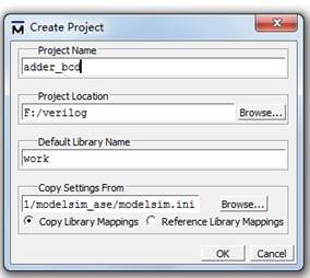
2. 创建一个新工程:①在主菜单窗口的主菜单中选择“File→New→Project”。②在项目名称域中输入工程名称(如adder_bcd),如下图所示。③单击Browse按钮选择工程文件存储的目录。④确认默认库名称为work,单击OK按钮。
3. 创建新设计的文件:①单击OK按钮接受工程设置后,在主窗口的工作区将出现一个工程标签,同时弹出向工程添加项目的对话框。单击“Create New File”,在新弹出的窗口中,输入文件名(如adder_1bit),特别需要注意的是,“Add file as type”里边要选择“verilog”类型。②如果还需要写新的模块,在project对话框中点右键,选择“Add to Project→New File”。在弹出的对话框中输入新的文件名(如adder_bcd_1bit;adder_bcd_4bit;test),同样注意“Add file as type”里边要选择“verilog”类型。


4. 向工程输入有效的设计单元:把设计的源文件输入到工程里边。
5. 在主窗口中选择“Compile→Compile All”完成工程的编译。对于modelsim正确编译的设计文件,都打上“√”标志;对于编译失败的情况,打上“×”标志,此时可在右侧的脚本状态窗中查看出错信息,修正后再编译。

6. 完成工程正确的编译后,在主窗口中单击Library标签,进入编译库页,打开work库,双击测试单元(如test),加载测试单元。对mycount点右键,选择“Add to wave”。然后就会出现Wave窗口,单击run就会运行并出现波形图。

7. 仿真结束时,在主菜单中选择“Simulate→End Simulate”,结束仿真。
3.2 本次所实现的功能描述
4位BCD加法器,1位BCD用4位二进制数来表示,故4位BCD相加应为16位2进制数相加。先写1位二进制加法器(adder_1bit),用与门实现。然后写1位BCD加法器(adder_bcd_1bit),即4位二进制加法器,把1位二进制加法器实例化四次。下来写4位BCD加法器(adder_bcd_4bit),把1位BCD加法器实例化四次。最后写测试模块(test)。
完成了16位二进制数相加。
3.3 本次实验的设计方案
module adder_1bit(a,b,cin,sum,cout);
input a,b,cin;
output sum,cout;
wire s1,m1,m2,m3;
and(m1,a,b),(m2,b,cin),(m3,a,cin);
xor(s1,a,b),(sum,s1,cin);
or(cout,m1,m2,m3);
endmodule
module adder_bcd_1bit(a,b,cin,sum,cout);
input[3:0]a,b;
input cin;
output[3:0]sum;
output cout;
wire cin1,cin2,cin3;
wire count;
wire [3:0] sum1;
adder_1bit f0(.a(a[0]),.b(b[0]),.cin(cin),.sum(sum1[0]),.cout(cin1));
adder_1bit f1(.a(a[1]),.b(b[1]),.cin(cin1),.sum(sum1[1]),.cout(cin2));
adder_1bit f2(.a(a[2]),.b(b[2]),.cin(cin2),.sum(sum1[2]),.cout(cin3));
adder_1bit f3(.a(a[3]),.b(b[3]),.cin(cin3),.sum(sum1[3]),.cout(count));
assign sum=((sum1>4'b1001)|(count==1'b1))?(sum1+4'd6):sum1;
assign cout=((sum1>4'b1001)|(count==1'b1))?1'b1:1'b0;
endmodule
module adder_bcd_4bit(a,b,cin,sum,cout);
input [15:0] a,b;
input cin;
output [15:0] sum;
output cout;
wire cin1,cin2,cin3;
wire [15:0] sum;
wire cout;
adder_bcd_1bit adder1(.a(a[3:0]),.b(b[3:0]),.cin(cin),.sum(sum[3:0]),.cout(cin1));
adder_bcd_1bit adder2(.a(a[7:4]),.b(b[7:4]),.cin(cin1),.sum(sum[7:4]),.cout(cin2));
adder_bcd_1bit adder3(.a(a[11:8]),.b(b[11:8]),.cin(cin2),.sum(sum[11:8]),.cout(cin3));
adder_bcd_1bit adder4(.a(a[15:12]),.b(b[15:12]),.cin(cin3),.sum(sum[15:12]),.cout(cout));
endmodule
module test;
reg [15:0] a,b;
reg cin;
wire [15:0] sum;
wire cout;
adder_bcd_4bit mytest(.a(a),.b(b),.cin(cin),.sum(sum),.cout(cout));
always #21 cin=~cin;
initial begin
a=16'b0;
b=16'b0;
cin=1'b0;
#7 a=16'b0000_0000_0000_0110;b=16'b0000_0000_0000_0101;
#7 a=16'b0000_0000_1100_0010;b=16'b0000_0000_0000_0010;
#7 a=16'b0000_1110_0000_0000;b=16'b0000_0110_0000_0000;
#7 a=16'b1010_0000_0000_0000;b=16'b0101_0000_0000_0000;
#7 a=16'b1001_0010_1100_0010;b=16'b0101_1010_0111_0101;
end
endmodule
3.4 本次实验设计的结果
①在主窗口中单击Library标签,进入编译库页,打开work库,双击测试单元test.

② 加载测试单元。对mytest点右键,选择“Add to wave”。

③ 后就会出现Wave窗口,单击run就会运行并出现波形图。

4.实验总结
此次实验使我进一步熟悉了modelsim仿真工具的使用。做了几个设计之后,现在也能熟练应用了,对moelsim有了基本的了解。
记得上次实验还不会写激励模块,但是这次实验已经能很轻松地写出来了。真的学会之后才发现,激励模块要比建模模块好写多了。难怪老师说激励模块很简单呢。
这次比上次的进步就是modelsim的使用更加熟练了,此外,上次出现的问题这次也没再出现了。当然,这次实验也有新的问题出现。其一,给同一个变量sum两次赋值,导致多驱动的发生。其二,assign语句等式左边的变量和实例化里边的变量要定义为wire类型。这是一个不该出现的问题,因为老师上课已经强调过了,我自己也做了笔记,可是还是出现这样的问题。听了是一方面,真正会应用是另外一方面,所以以后一定要多动手,真正会使用才算把知识学到手。其三,课前准备工作一定要做好,务必要把此次实验所要仿真的设计设计好。实验课课堂上是让你使用modelsin编译仿真的,没有时间再去设计。所以以后一定要注意,课前把设计写好。
第二篇:四位加法器实验报告
四位加法器实验报告
1.实验目的:
掌握组合逻辑电路的基本分析与设计方法;
理解半加器和全加器的工作原理并掌握利用全加器构成不同字长加法器的各种方法;
学习元件例化的方式进行硬件电路设计;
学会利用软件仿真实现对数字电路的逻辑功能进行验证和分析。
2.实验仪器:
数字逻辑实验箱
3.实验内容:
A. 设计实现逐次进位加法器,进行软件仿真并在实验平台上测试。
B. 设计实现超前进位加法器,进行软件仿真并在实验平台上测试。
C.使用VHDL自带加法运算实现一个4位全加器。
4.实验代码:
A. 逐次进位加法器:
library ieee;
use ieee.std_logic_1164.all;
use ieee.std_logic_unsigned.all;
entity FDFA is #定义串行加法器总体接口
port(
A,B:in std_logic_vector(3 downto 0);
Ci:in std_logic;
S:out std_logic_vector(3 downto 0);
Co:out std_logic);
end entity;
architecture struct of FDFA is
component fadder is #基于一位全加器
port(
a,b,ci:in std_logic;
s,co:out std_logic);
end component fadder;
signal c0,c1,c2:std_logic;
begin
U0:fadder port map(A(0),B(0),Ci,S(0),c0);
U1:fadder port map(A(1),B(1),c0,S(1),c1);
U2:fadder port map(A(2),B(2),c1,S(2),c2);
U3:fadder port map(A(3),B(3),c2,S(3),Co);
end architecture struct;
library ieee;
use ieee.std_logic_1164.all;
use ieee.std_logic_unsigned.all;
entity fadder is #定义一位全加器
port(
a,b,ci:in std_logic;
s,co:out std_logic);
end entity;
architecture func of fadder is
begin
co<=(a and b) or (ci and ( a xor b));
s<=a xor b xor ci;
end architecture func;
B. 超前进位加法器:
library ieee;
use ieee.std_logic_1164.all;
use ieee.std_logic_unsigned.all;
entity LAC is #定义超前进位加法器总体接口
port(
A,B:in std_logic_vector(3 downto 0);
Ci:in std_logic;
Co:out std_logic;
S:out std_logic_vector(3 downto 0)
);
end entity;
architecture struct of LAC is
signal wirep, wireg:std_logic_vector(3 downto 0);
signal wirec:std_logic_vector(2 downto 0);
component fadder is #基于一位全加器
port(
Ai,Bi:in std_logic;
c:in std_logic;
si:out std_logic;
pi:out std_logic;
gi:out std_logic
);
end component fadder;
component Ker is #Ker总理进位传递信号P与进位产生信号G,以及进位信号C
port(
ci:in std_logic;
P:in std_logic_vector(3 downto 0);
G:in std_logic_vector(3 downto 0);
C:out std_logic_vector(3 downto 0)
);
end component Ker;
begin
U0:fadder port map(Ai=>A(0),Bi=>B(0),c=>Ci,si=>S(0),pi=>wirep(0),gi=>wireg(0));
U1:fadder port map(Ai=>A(1),Bi=>B(1),c=>wirec(0),si=>S(1),pi=>wirep(1),gi=>wireg(1));
U2:fadder port map(Ai=>A(2),Bi=>B(2),c=>wirec(1),si=>S(2),pi=>wirep(2),gi=>wireg(2));
U3:fadder port map(Ai=>A(3),Bi=>B(3),c=>wirec(2),si=>S(3),pi=>wirep(3),gi=>wireg(3));
L:Ker port map(ci=>Ci,P(0)=>wirep(0),P(1)=>wirep(1),P(2)=>wirep(2),P(3)=>wirep(3),G(0)=>wireg(0),G(1)=>wireg(1),G(2)=>wireg(2),G(3)=>wireg(3),C(0)=>wirec(0),C(1)=>wirec(1),C(2)=>wirec(2),C(3)=>Co);
end architecture struct;
library ieee;
use ieee.std_logic_1164.all;
use ieee.std_logic_unsigned.all;
entity fadder is #定义一位全加器
port(
Ai,Bi:in std_logic;
c:in std_logic;
si:out std_logic;
pi:out std_logic;
gi:out std_logic
);
end entity;
architecture func of fadder is
begin
pi<=Ai xor Bi;
gi<=Ai and Bi;
si<=Ai xor Bi xor c;
end architecture func;
library ieee;
use ieee.std_logic_1164.all;
use ieee.std_logic_unsigned.all;
entity Ker is #定义Ker
port(
ci:in std_logic;
P:in std_logic_vector(3 downto 0);
G:in std_logic_vector(3 downto 0);
C:out std_logic_vector(3 downto 0)
);
end entity;
architecture func of Ker is
begin
C(0)<=G(0) or ( P(0) and ci );
C(1)<=G(1) or ( P(1) and G(0) ) or ( P(1) and P(0) and ci );
C(2)<=G(2) or ( P(2) and G(1) ) or ( P(2) and P(1) and G(0) ) or ( P(2) and P(1) and P(0) and ci );
C(3)<=G(3) or ( P(3) and G(2) ) or ( P(3) and P(2) and G(1) ) or ( P(3) and P(2) and P(1) and G(0) ) or ( P(3) and P(2) and P(1) and P(0) and ci );
end architecture func;
C. VHDL自带加法运算实现4位全加器:
library ieee;
use ieee.std_logic_1164.all;
use ieee.std_logic_unsigned.all;
entity VHDLAD is #定义VHDL自带加法运算实现4位全加器总体接口,如果加和比原来和少,则会进位
port(
A,B:in std_logic_vector(3 downto 0);
Ci:in std_logic;
Co:out std_logic;
S:out std_logic_vector(3 downto 0));
end VHDLAD;
architecture bhv of VHDLAD is
signal D:std_logic_vector(3 downto 0);
begin
process(A,B,Ci,D)
begin
D <= A + B;
if(Ci = '1') then
D <= D + 1;
end if;
if(D >= A) then
S <= D;
Co <= '0';
else
S <= D;
Co <= '1';
end if;
end process;
end bhv;
5.软件仿真结果
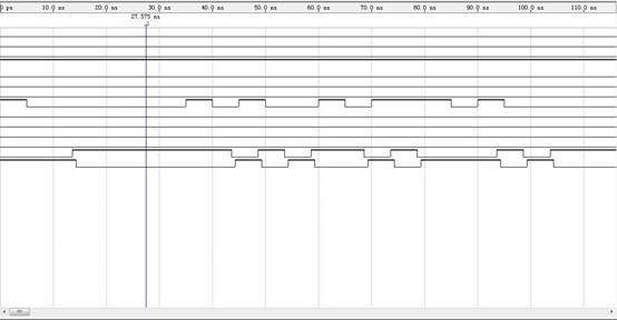
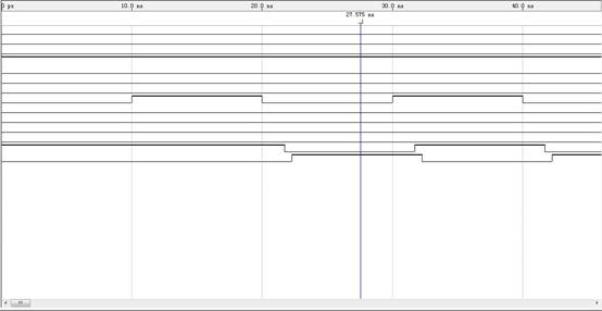
说明下面图片每幅有14条信号线,从上到下依次为A的低位到高位(共4条)、B的低位到高位(共4条)、输入的进位信号、和的低位到高位(共4条)、输出进位信号。
A. 逐次进位加法器:

短时间,延时明显

长时间,延时不明显
B. 超前进位加法器:
短时间,延时明显

长时间,延时不明显
C. VHDL自带加法运算实现4位全加器:
短时间,延时明显

长时间,延时不明显
6.电路功能测试结果
完全按照设计的逻辑功能,延时感觉并不明显。
7.实验总结
3种设计的延时差异并不明显,实验过程中遇到的最大问题是多个component的通信问题,可以通过设置signal解决这一问题。
-
Verilog实验报告(电子)
西安邮电大学VerilogHDL大作业报告书学院名称学生姓名专业名称班级电子工程学院电子信息工程实验一异或门设计一实验目的1熟悉M…
-
Verilog 实验报告
实验一简单组合逻辑电路的设计一实验要求1用verilogHDL语言描写出简单的一位数据比较器及其测试程序2用测试程序对比较器进行波…
-
北航verilog实验报告
北京航空航天大学电子电路设计数字部分实验报告实验一简单组合逻辑设计2实验二简单分频时序逻辑电路的设计3一实验目的1掌握最基本组合逻…
-
Verilog实验报告
实验报告格式要求一实验报告内容包括1实验名称2实验目的3实验仪器及编号写明仪器名称型号编号4实验原理简单叙述有关实验原理包括电路图…
-
Verilog HDL 实验报告
实验一Modelsim仿真软件的使用一实验目的1熟悉Modelsim软件2掌握Modelsim软件的编译仿真方法3熟练运用Mode…
-
北航verilog实验报告
北京航空航天大学电子电路设计数字部分实验报告实验一简单组合逻辑设计2实验二简单分频时序逻辑电路的设计3一实验目的1掌握最基本组合逻…
-
Verilog期末实验报告—波形发生器
深圳大学实验报告课程名称:Verilog使用及其应用实验名称:频率可变的任意波形发生器学院:电子科学与技术学院专业:电子科学与技术…
-
Verilog HDL 实验报告
实验一Modelsim仿真软件的使用一实验目的1熟悉Modelsim软件2掌握Modelsim软件的编译仿真方法3熟练运用Mode…
-
verilog电子钟实验报告
深圳大学实验报告课程名称硬件描述语言与逻辑综合实验项目名称电子时钟VerilogHDL的设计与仿真学院电子科学与技术学院专业微电子…
-
Verilog实验报告(电子)
西安邮电大学VerilogHDL大作业报告书学院名称学生姓名专业名称班级电子工程学院电子信息工程实验一异或门设计一实验目的1熟悉M…
-
EDA实验报告(四选一、四位比较器、加法器、计数器、巴克码发生器)
EDA实验报告姓名学号班级实验14选1数据选择器的设计一实验目的1学习EDA软件的基本操作2学习使用原理图进行设计输入3初步掌握器…