dsp实验报告
DSP实验报告
院系名称 电气与信息工程学院
专业名称 电气工程及其自动化
班 级 电气1002班
学生姓名 苏 美 龙
学 号 10401700403
指导老师 易 吉 良
2013年 11 月 6 日
实验一 拨码开关实验
—、实验目的
1.了解DSP开发系统的组成和结构
2.了解IO 的基本编程方法
二、实验设备
计算机,CCS3.1版本软件,DSP 仿真器,E300 实验箱,2812CPU板(新的)
三、实验原理
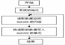
8位的数字量输入(由拨码开关产生),当拨码打到靠近LED时为低。相反为高。通过74LS244(可读)缓冲连接到DSP 的数据总线的低8 位。CPU 通过读指令读取到拨码开关产生的8 位输出的数字量,然后CPU通过写指令把读出的8 位数字量写入(0x0200)单元内,使连接到DSP的数据总线的低8 位的74LS273的输出端产生高低信号,此时LED 灯产生亮灭。当对应LED 灯点亮时说明输出为低,熄灭时为高。(器件 74LS244和74LS273详细的介绍请参看数据手册)。
数字量输入输出单元的资源分配如下:
基地址:0000h(当CS0为0时分配有效)
数字量分配空间为数据空间地址:基地址+0x200(低8位,只读)
拨码开关扩展工作原理

说明:74LS244 片选号、74LS273 片选信号和74LS273 复位信号由E300 上CPLD 译码产生。
本实验使用DSP 数据总线的低8位。
本实验的程序流程框图如下:
四、实验步骤
1. 2812CPU板上的JUMP1的1和2脚短接,拨码开关SW1的第二位置ON。
2.E300 板上的开关SW4 的第一位置ON,其余OFF;SW5开关全部置ON;其余开关全部置OFF。
3. 运行Code Composer Studio (CCS)(ccs3.1需要“DEBUG→Connect” )
4. 用“Project\Open”打开系统项目文件\e300.test \ normal\DSP2801x_example\e300_02_swich\ Exampla_281_swich.pjt;
5. 编译全部文件并装载\normal\DSP2801x_example\e300_02_swich\ Exampla_281_swich.out;
6. 单击“Debug \Go Main”跳到主程序的开始;
7. 单击“Debug \RUN”运行程序
8.任意拨动E300 底板上的拨动开关,观察LED和拨动开关的对应情况。(LED1-LED7分别对应DSP 数据总线的D0-D7);
9.单击“Debug \Halt” 暂停持续运行,开关将对灯失去控制.
10.关闭所有窗口,本实验完。
五、实验结果
设置好CCS的环境,打开本工程,编译、下载、运行。调整数字输入输出单元的开关K1~K8,观察LED1~LED8灯亮灭的变化为:拨动LED1~LED8灯相应的开关K1~K8,则对应的灯亮灭。
修改后的实验原程序:
#include "DSP281x_Device.h" // DSP281x Headerfile Include File
#include "DSP281x_Examples.h" // DSP281x Examples Include File
void main(void)
{
unsigned int temp;
temp = 0;
InitSysCtrl();//初始化PLL,WatchDog,使能外围时钟,该初始化文件在"DSP281x_SysCtrl.c"中
DINT;//关闭CPU中断
InitPieCtrl();
IER = 0x0000;//关闭中断和清除所有中断标志
IFR = 0x0000;
InitPieVectTable();
for(;;)
{
asm(" nop ");
temp = *(int *)0x2200&0x0007; //读入0x2200地址的开关量值并赋给temp
switch(temp)
{
case 0x0000: * (int *)0x2200 = 0x00fe; break;
case 0x0001: * (int *)0x2200 = 0x00fd; break;
case 0x0002: * (int *)0x2200 = 0x00fb; break;
case 0x0003: * (int *)0x2200 = 0x00f7; break;
case 0x0004: * (int *)0x2200 = 0x00ef; break;
case 0x0005: * (int *)0x2200 = 0x00df; break;
case 0x0006: * (int *)0x2200 = 0x00bf; break;
case 0x0007: * (int *)0x2200 = 0x007f; break;
default:break;
}
asm(" nop ");
asm(" nop ");
}
}
实验二 定时器实验
一、实验目的
1、熟悉F2812的CPU定时器;
2、掌握F2812的CPU定时器的控制方法;
3、学会使用CUP定时器中断方式控制程序流程。二、实验设备
计算机,CCS3.1版软件,DSP硬件仿真器,E300实验箱,2812CPU板。
三、实验原理说明
样例实验是采用CPU定时器来定时LED亮灭的。
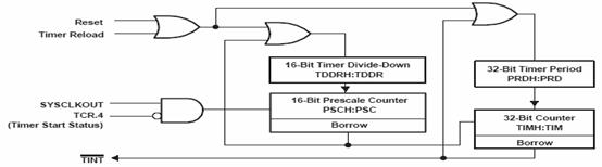
F2812的CPU定时器不同于事件管理器(EVA\EVB)中的通用定时器(GP)。F2812的CPU共有三个定时器,其中,CPU1定时器1和2被保留用作实验操作系统OS例如DSPBIOS),CPU定时器0可以供用户使用。
定时器的一般操作如下:将周期寄存器PRDH:PRD中的值装入32位计数器寄存器TIMI:TIM。然后计数器寄存器以F2812x的SYSCLKLT速率递减。当计数器减到0,就会产生一个定时器中断输出定时信号(一个中断脉冲)。
下图为CPU定时器的内部结构:
样例实验的程序如下:
四、实验步骤和内容
1、F2812CPU板的JUPMI的1和2脚短接,拨码开关 SW1的第二位置ON;其余OFF。
2、E300 底板的开关SW4 的第1位置ON,其余位置OFF。其余开关设置为OFF;
3、运行CCS软件,调入样例程序,装载并运行;(进入CCS界面后需要点“Debug--Connect”);
4、加载“..\e300_03cpu_timer\Debug\Eample_281x_cpu_timer.out”;
单击“Debug \ Animate”运行,
可观察到LED1~LED8的变化规律:
先LED1,8点亮—LED2,7D点亮—LED1,8熄灭—LED3,6点亮—LED2,7熄灭—LED4,5点亮—LED3,6熄灭—后LED4,5熄灭—LED3,6点亮—LED3,6熄灭—LED2,7点亮—LED2,7熄灭—LED1,8点亮。
6、单击“Debug \ Halt”,暂停程序运行,LED灯停止闪烁;单击“RUN”,LED灯又开始闪烁变化;
7、结束试验程序
8、修改后的实验原程序:
#include "DSP281x_Device.h"
#include "DSP281x_Examples.h"
interrupt void cpu_timer0_isr(void);
void ConfigCpuTimer(struct CPUTIMER_VARS *Timer, float Freq, float Period);
void main(void)
{
unsigned int temp;
temp = 0;
InitSysCtrl();
DINT;
InitPieCtrl();
IER = 0x0000;
IFR = 0x0000;
InitPieVectTable();
EALLOW;
PieVectTable.TINT0 = &cpu_timer0_isr;
EDIS;
InitCpuTimers();
ConfigCpuTimer(&CpuTimer0, 100, 100000);
StartCpuTimer0();
IER |= M_INT1;
PieCtrlRegs.PIEIER1.bit.INTx7 = 1;
EINT;
ERTM;
for(;;)
{
temp = *(int *)0x2200&0x0001;
if (temp==0)
{
if(CpuTimer0.InterruptCount<1)
{
asm(" nop ");
asm(" nop ");
*(int *)0x2200=0x00fe;
*(int *)0x2200=0x007f;
}
else if(CpuTimer0.InterruptCount<2)
{
asm(" nop ");
asm(" nop ");
*(int *)0x2200=0x00fe;
*(int *)0x2200=0x007f;
*(int *)0x2200=0x00fd;
*(int *)0x2200=0x00bf;
}
else if(CpuTimer0.InterruptCount<3)
{
asm(" nop ");
asm(" nop ");
*(int *)0x2200=0x00fd;
*(int *)0x2200=0x00bf;
}
else if(CpuTimer0.InterruptCount<4)
{
asm(" nop ");
asm(" nop ");
*(int *)0x2200=0x00fd;
*(int *)0x2200=0x00bf;
*(int *)0x2200=0x00fb;
*(int *)0x2200=0x00df;
}
else if(CpuTimer0.InterruptCount<5)
{
asm(" nop ");
asm(" nop ");
*(int *)0x2200=0x00fb;
*(int *)0x2200=0x00df;
}
else if(CpuTimer0.InterruptCount<6)
{
asm(" nop ");
asm(" nop ");
*(int *)0x2200=0x00fb;
*(int *)0x2200=0x00df;
*(int *)0x2200=0x00f7;
*(int *)0x2200=0x00ef;
}
else if(CpuTimer0.InterruptCount<7)
{
asm(" nop ");
asm(" nop ");
*(int *)0x2200=0x00f7;
*(int *)0x2200=0x00ef;
}
else if(CpuTimer0.InterruptCount<8)
{
asm(" nop ");
asm(" nop ");
*(int *)0x2200=0x00ff;
}
else if(CpuTimer0.InterruptCount<9)
{
asm(" nop ");
asm(" nop ");
*(int *)0x2200=0x00fb;
*(int *)0x2200=0x00df;
}
else if(CpuTimer0.InterruptCount<10)
{
asm(" nop ");
asm(" nop ");
*(int *)0x2200=0x00ff;
}
else if(CpuTimer0.InterruptCount<11)
{
asm(" nop ");
asm(" nop ");
*(int *)0x2200=0x00fd;
*(int *)0x2200=0x00bf;
}
else if(CpuTimer0.InterruptCount<12)
{
asm(" nop ");
asm(" nop ");
*(int *)0x2200=0x00ff;
}
else
{
CpuTimer0.InterruptCount = 0;
}
}
else if (temp==1)
{
if(CpuTimer0.InterruptCount<9)
{
asm(" nop ");
asm(" nop ");
*(int *)0x2200=0x00fe;
*(int *)0x2200=0x007f;
}
else if(CpuTimer0.InterruptCount<8)
{
asm(" nop ");
asm(" nop ");
*(int *)0x2200=0x00fe;
*(int *)0x2200=0x007f;
*(int *)0x2200=0x00fd;
*(int *)0x2200=0x00bf;
}
else if(CpuTimer0.InterruptCount<3)
{
asm(" nop ");
asm(" nop ");
*(int *)0x2200=0x00fd;
*(int *)0x2200=0x00bf;
}
else if(CpuTimer0.InterruptCount<4)
{
asm(" nop ");
asm(" nop ");
*(int *)0x2200=0x00fd;
*(int *)0x2200=0x00bf;
*(int *)0x2200=0x00fb;
*(int *)0x2200=0x00df;
}
else if(CpuTimer0.InterruptCount<5)
{
asm(" nop ");
asm(" nop ");
*(int *)0x2200=0x00fb;
*(int *)0x2200=0x00df;
}
else if(CpuTimer0.InterruptCount<6)
{
asm(" nop ");
asm(" nop ");
*(int *)0x2200=0x00fb;
*(int *)0x2200=0x00df;
*(int *)0x2200=0x00f7;
*(int *)0x2200=0x00ef;
}
else if(CpuTimer0.InterruptCount<7)
{
asm(" nop ");
asm(" nop ");
*(int *)0x2200=0x00f7;
*(int *)0x2200=0x00ef;
}
else if(CpuTimer0.InterruptCount<8)
{
asm(" nop ");
asm(" nop ");
*(int *)0x2200=0x00ff;
}
else if(CpuTimer0.InterruptCount<9)
{
asm(" nop ");
asm(" nop ");
*(int *)0x2200=0x00fb;
*(int *)0x2200=0x00df;
}
else if(CpuTimer0.InterruptCount<10)
{
asm(" nop ");
asm(" nop ");
*(int *)0x2200=0x00ff;
}
else if(CpuTimer0.InterruptCount<11)
{
asm(" nop ");
asm(" nop ");
*(int *)0x2200=0x00fd;
*(int *)0x2200=0x00bf;
}
else if(CpuTimer0.InterruptCount<12)
{
asm(" nop ");
asm(" nop ");
*(int *)0x2200=0x00ff;
}
else
{
CpuTimer0.InterruptCount = 0;
}
}
}
}
interrupt void cpu_timer0_isr(void)
{
CpuTimer0.InterruptCount++;
PieCtrlRegs.PIEACK.all = PIEACK_GROUP1;
}
实验三 键盘接口实验(E300)
—、实验目的
1. 了解DSP开发系统的组成和结构
2. 了解键盘的基本编程方法
3. 内存观察工具的使用
二、实验设备
计算机,CCS3.1版本软件,DSP 仿真器,E300 实验箱,2812CPU板
三、实验原理
本实验程序由二部分组成:
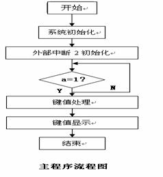
1.由外部中断2产生中断信号
2.键值读取程序:该部分有两种方法进行键值的判断。
方法1:利用内存观察工具进行观察
方法2:利用LED1-LED8 的亮灭对应显示键值。
a) 外部中断2的应用参照实验二;
b) 内存观察键值:程序中定义了三个变量“W”“row”和“col”。“W”代表是CPLD 中键盘的扫描数值,“row”和“col”分别代表键盘的行和列,由行和列可以判定按键的位置。上述三个变量可以在观察窗口中观察的。
c) 利用LED 灯显示键值原理,参看实验一。具体的LED 灯显示值以查表的形式读出,请参看“e300_codec.h”库文件。
本实验的CPLD地址译码说明:
基地址:0x2000,当底板片选CS1为低时,分配有效。
CPU的数据空间:基地址+0x0200 LED灯 output8
外部中断用XINT2:由CPLD分配,中断信号由键盘产生。
中断下降沿触发。
KEY_DAY_REG(R):基地址+0x0004;
四、实验步骤和内容
1. 2812CPU板JUMP1的1和2脚短接,拨码开关SW1的第二位ON;
2.E300 板上的开关SW4 的第一位置ON,其余OFF;SW3 的第四位置ON 其余的SW 置OFF;
3.运行Code Composer Studio (CCS)(ccs3.1需要“DEBUG→Connect” );
4.打开系统项目文件\e300.test\ normal\ DSP281x_examples\e300_06_key interface \Example_281x_ keyled.pjt;
5.编译全部文件并装载“\Debug\ keyled.out”文件;
6.单击“Debug\Go Main”跳到主程序的开始;
7.指定位置设置断点;
8.View--〉Watch Window 打开变量观察窗口;
将变量“w”“ row”和“ col”添加到观察窗口中,改变变量观察窗口的显示方式为HEX 显示;
点击“Debug--〉Animate”全速运行,然后点击E300 板上键盘按键,观察窗口中变量变化,同时LED1-LED8 灯也相应变化,指示键值。(注意程序中KEY_E和KEY_F分别代表键盘上的“*”和“#”键值。十六进制数代表的意义为:高4 位为按键的行值,低4 位为按键的列值。注意:“w”中的低八位表;
11.关闭所有窗口,本实验完毕。
五、实验程序框图
修改后的实验原程序:
#include "DSP281x_Device.h" // DSP281x Headerfile Include File
#include "DSP281x_Examples.h" // DSP281x Examples Include File
#include "e300_codec.h"
void init_xint2(void);
interrupt void xint2_isr(void); //中断2中断子程序
void read_data ();//读取数据子函数
void conv(void);//键盘数值转换子函数
interrupt void cpu_timer0_isr(void);
void ConfigCpuTimer(struct CPUTIMER_VARS *Timer, float Freq, float Period);
unsigned int row,col,w;
int a=0;
unsigned int temp=0;
void init_xint2()
{
XIntruptRegs.XINT2CR.all=0x0001; //低电平触发中断
}
interrupt void xint2_isr() //中断2中断子程序
{
a=1;
//开总中断
PieCtrlRegs.PIEACK.all = PIEACK_GROUP1;
}
interrupt void cpu_timer0_isr(void)
{
CpuTimer0.InterruptCount++;
more interrupts from group 1
PieCtrlRegs.PIEACK.all = PIEACK_GROUP1;
}
void main(void)
{
Clocks
DSP281x_SysCtrl.c file.
InitSysCtrl();
DINT;
default state.
disabled and flags
InitPieCtrl();
CPU interrupt flags:
IER = 0x0000;
IFR = 0x0000;
to the shell Interrupt
InitPieVectTable();
EALLOW; // This is needed to write to EALLOW protected registers
PieVectTable.XINT2 = &xint2_isr;
PieVectTable.TINT0 = &cpu_timer0_isr;
EDIS;
InitCpuTimers(); // For this example, only initialize the Cpu Timers
second:
uSeconds)
ConfigCpuTimer(&CpuTimer0, 100, 100000);
StartCpuTimer0();
init_xint2();
PieCtrlRegs.PIEIER1.all = 0x0050;
IER |= M_INT1 ;
EINT; // Enable Global interrupt INTM
ERTM; // Enable Global realtime interrupt DBGM
for(;;)
{
if(a==1)//加软件断点
{
temp = *(int *)0x2200&0x0001;
if (temp==0)
{
if(CpuTimer0.InterruptCount<1)
{
asm(" nop ");
asm(" nop ");
*(int *)0x2200=0x00fe;
*(int *)0x2200=0x007f;
}
else if(CpuTimer0.InterruptCount<2)
{
asm(" nop ");
asm(" nop ");
*(int *)0x2200=0x00fe;
*(int *)0x2200=0x007f;
*(int *)0x2200=0x00fd;
*(int *)0x2200=0x00bf;
}
else if(CpuTimer0.InterruptCount<3)
{
asm(" nop ");
asm(" nop ");
*(int *)0x2200=0x00fd;
*(int *)0x2200=0x00bf;
}
else if(CpuTimer0.InterruptCount<4)
{
asm(" nop ");
asm(" nop ");
*(int *)0x2200=0x00fd;
*(int *)0x2200=0x00bf;
*(int *)0x2200=0x00fb;
*(int *)0x2200=0x00df;
}
else if(CpuTimer0.InterruptCount<5)
{
asm(" nop ");
asm(" nop ");
*(int *)0x2200=0x00fb;
*(int *)0x2200=0x00df;
}
else if(CpuTimer0.InterruptCount<6)
{
asm(" nop ");
asm(" nop ");
*(int *)0x2200=0x00fb;
*(int *)0x2200=0x00df;
*(int *)0x2200=0x00f7;
*(int *)0x2200=0x00ef;
}
else if(CpuTimer0.InterruptCount<7)
{
asm(" nop ");
asm(" nop ");
*(int *)0x2200=0x00f7;
*(int *)0x2200=0x00ef;
}
else if(CpuTimer0.InterruptCount<8)
{
asm(" nop ");
asm(" nop ");
*(int *)0x2200=0x00ff;
}
else if(CpuTimer0.InterruptCount<9)
{
asm(" nop ");
asm(" nop ");
*(int *)0x2200=0x00fb;
*(int *)0x2200=0x00df;
}
else if(CpuTimer0.InterruptCount<10)
{
asm(" nop ");
asm(" nop ");
*(int *)0x2200=0x00ff;
}
else if(CpuTimer0.InterruptCount<11)
{
asm(" nop ");
asm(" nop ");
*(int *)0x2200=0x00fd;
*(int *)0x2200=0x00bf;
}
else if(CpuTimer0.InterruptCount<12)
{
asm(" nop ");
asm(" nop ");
*(int *)0x2200=0x00ff;
}
else
{
CpuTimer0.InterruptCount = 0;
}
}
else if (temp==1)
{
if(CpuTimer0.InterruptCount<9)
{
asm(" nop ");
asm(" nop ");
*(int *)0x2200=0x00fe;
*(int *)0x2200=0x007f;
}
else if(CpuTimer0.InterruptCount<8)
{
asm(" nop ");
asm(" nop ");
*(int *)0x2200=0x00fe;
*(int *)0x2200=0x007f;
*(int *)0x2200=0x00fd;
*(int *)0x2200=0x00bf;
}
else if(CpuTimer0.InterruptCount<3)
{
asm(" nop ");
asm(" nop ");
*(int *)0x2200=0x00fd;
*(int *)0x2200=0x00bf;
}
else if(CpuTimer0.InterruptCount<4)
{
asm(" nop ");
asm(" nop ");
*(int *)0x2200=0x00fd;
*(int *)0x2200=0x00bf;
*(int *)0x2200=0x00fb;
*(int *)0x2200=0x00df;
}
else if(CpuTimer0.InterruptCount<5)
{
asm(" nop ");
asm(" nop ");
*(int *)0x2200=0x00fb;
*(int *)0x2200=0x00df;
}
else if(CpuTimer0.InterruptCount<6)
{
asm(" nop ");
asm(" nop ");
*(int *)0x2200=0x00fb;
*(int *)0x2200=0x00df;
*(int *)0x2200=0x00f7;
*(int *)0x2200=0x00ef;
}
else if(CpuTimer0.InterruptCount<7)
{
asm(" nop ");
asm(" nop ");
*(int *)0x2200=0x00f7;
*(int *)0x2200=0x00ef;
}
else if(CpuTimer0.InterruptCount<8)
{
asm(" nop ");
asm(" nop ");
*(int *)0x2200=0x00ff;
}
else if(CpuTimer0.InterruptCount<9)
{
asm(" nop ");
asm(" nop ");
*(int *)0x2200=0x00fb;
*(int *)0x2200=0x00df;
}
else if(CpuTimer0.InterruptCount<10)
{
asm(" nop ");
asm(" nop ");
*(int *)0x2200=0x00ff;
}
else if(CpuTimer0.InterruptCount<11)
{
asm(" nop ");
asm(" nop ");
*(int *)0x2200=0x00fd;
*(int *)0x2200=0x00bf;
}
else if(CpuTimer0.InterruptCount<12)
{
asm(" nop ");
asm(" nop ");
*(int *)0x2200=0x00ff;
}
else
{
CpuTimer0.InterruptCount = 0;
}
}
read_data();
// conv();
}
else {}
}
}
六、实验建议
本实验程序采用外部中断的方式来判断键盘是否被按下,除了这种方法外,还可以根据键盘按下标志位“KEY_FLAG”,利用查询方式来编写程序,“KEY_FLAG”是CPLD内部状态寄存器中的一个只读位.
CPLD内部状态寄存器:
CPLD_ST
实验四 A/D转换实验(E300)
一、实验目的
1. 了解DSP 中A/D转换模块的特点;
2. 了解A/D转换模块的原理结构;
3. 掌握A/D转换模块的使用。
二、实验设备
计算机,DSP仿真器,THRSC-2型实验箱各一台。
三、实验原理
TMS320F2812的ADC模块是一个12位分辨率、高达80ns转换时间、具有流水线结构的模
—数转换器。此转换器的模拟电路包括:前端模拟多路复用器(MUXs)、采样/保持电路(S/H)、
转换核、电压调节器以及其他模拟支持电路。数字电路包括:可编程转换序列发生器、转换结果
寄存器、模拟电路接口、设备外围总线接口以及其他片上模块接口等,可以直接用于电机或运动
控制场合。
四、实验内容与步骤
连接好仿真器、计算机与实验箱,系统上电,实验箱电源指示灯亮,仿真器上红色指示灯亮,
系统连接正常。打开CCS3.1软件。
图1.6.3 实验程序流程图
1.图1.6.3为A/D实验程序流程图:采集电位器电压。A/D用16个通道采集当前电压值,
取平均值,将十六进制数转换成十进制数,并处理成电压量输出给液晶屏显示,循环上述操作。
2.打开实验程序dsp2812.1.6-ADC目录下的工程ADC.pjt,点 编译、下载。按“F5”运
行,液晶屏显示当前DSP的ADCINA2(对应试验箱A/D转换单元的ADCINA)通道电压值,
调节A/D转换单元的电位器,改变输入电压,显示随之变化,显示电压在0~3.3V之间。
3.点“Halt”,停止程序运行,恢复程序指令初始值,并保存,关闭所有窗口,实验完毕。
修改后的实验原程序:
#include "DSP281x_Device.h" // DSP281x Headerfile Include File
#include "DSP281x_Examples.h" // DSP281x Examples Include File
interrupt void adc_isr(void);
Uint16 LoopCount;
Uint16 ConversionCount;
double input1[256];
double input2[256];
Uint16 a[4],b[4];
Uint16 sum1=0,sum2=0
void main(void)
{
InitSysCtrl();
EALLOW;
SysCtrlRegs.PLLCR.all=0x8;
SysCtrlRegs.HISPCP.all = 0x3; // HSPCLK = SYSCLKOUT/6
EDIS;
DINT;
InitPieCtrl();
IER = 0x0000;
IFR = 0x0000;
InitPieVectTable();
EALLOW; // This is needed to write to EALLOW protected register
PieVectTable.ADCINT = &adc_isr;
EDIS; // This is needed to disable write to EALLOW protected registers
InitAdc(); // For this example, init the ADC
PieCtrlRegs.PIEIER1.bit.INTx6 = 1;
IER |= M_INT1; // Enable CPU Interrupt 1
EINT; // Enable Global interrupt INTM
ERTM; // Enable Global realtime interrupt DBGM
LoopCount = 0;
ConversionCount = 0;
AdcRegs.ADCTRL1.bit.SEQ_CASC = 1;
AdcRegs.ADCMAXCONV.all = 0x0007; // Setup 2 conv's on SEQ1
AdcRegs.ADCCHSELSEQ1.bit.CONV00 = 0x0; // Setup ADCINA0 as 1st SEQ1 conv.
AdcRegs.ADCCHSELSEQ1.bit.CONV01 = 0x0; // Setup ADCINA2 as 2nd SEQ1 conv.
AdcRegs.ADCCHSELSEQ1.bit.CONV02 = 0x0;
AdcRegs.ADCCHSELSEQ1.bit.CONV03 = 0x0;
AdcRegs.ADCCHSELSEQ2.bit.CONV04 = 0x2;
AdcRegs.ADCCHSELSEQ2.bit.CONV05 = 0x2;
AdcRegs.ADCCHSELSEQ2.bit.CONV06 = 0x2;
AdcRegs.ADCCHSELSEQ2.bit.CONV07 = 0x2;
AdcRegs.ADCTRL2.bit.EVA_SOC_SEQ1 = 1; // Enable EVASOC to start SEQ1
AdcRegs.ADCTRL2.bit.INT_ENA_SEQ1 = 1; // Enable SEQ1 interrupt (every EOS)
EvaRegs.T1CMPR = 0x0380; // Setup T1 compare value
EvaRegs.T1PR = 0x07FF; // Setup period register
EvaRegs.GPTCONA.bit.T1TOADC = 1; // Enable EVASOC in EVA 01下溢中断启动ADC
EvaRegs.T1CON.all = 0x1042; // Enable timer 1 compare (upcount mode)
for(;;)
{
*(int *)0x2200=0x0005;
LoopCount++;
}
}
interrupt void adc_isr(void)
Uint16 i; // ,j
a[0]=AdcRegs.ADCRESULT0>>4;
a[1]=AdcRegs.ADCRESULT1>>4;
a[2]=AdcRegs.ADCRESULT2>>4;
a[3]=AdcRegs.ADCRESULT3>>4;
b[0]=AdcRegs.ADCRESULT4>>4;
b[1]=AdcRegs.ADCRESULT5>>4;
b[2]=AdcRegs.ADCRESULT6>>4;
b[3]=AdcRegs.ADCRESULT7>>4;
for(i=0;i<4;i++)
{
sum1=sum1+a[i];
sum1=sum1/2;
}
for(i=0;i<4;i++)
{
sum2=sum2+b[i];
sum2=sum2/2;
}
input1[ConversionCount] =sum1/4095.0*3;
input2[ConversionCount] =sum2/4095.0*3;
if(ConversionCount == 256)
{
ConversionCount = 0;//加软件断点
}
else ConversionCount++;
AdcRegs.ADCTRL2.bit.RST_SEQ1 = 1; // Reset SEQ1
AdcRegs.ADCST.bit.INT_SEQ1_CLR = 1; // Clear INT SEQ1 bit
PieCtrlRegs.PIEACK.all = PIEACK_GROUP1; // Acknowledge interrupt to PIE
return;
}
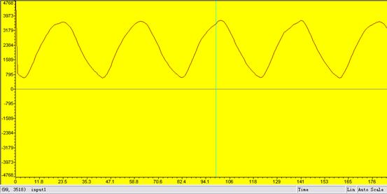
实验结果波形:
实验五 PWM波形产生实验
一、实验目的
1.了解PWM波的产生原理;
2.掌握PWM波的使用方法。
二、实验设备
计算机,DSP仿真器,THRSC-2型实验箱,示波器,电机扩展板
三、实验原理
1.事件管理器EVA模块和EVB模块中分别有3个全比较单元,EVA的3个全比较单元为:
比较单元1、2和3;EVB的3个全比较单元为:比较单元4、5和6。每个比较单元都有两个相
应的PWM输出。比较单元的时基由通用定时器1(EVA模块)和通用定时器3(EVB模块)提
供。当比较操作使能时,GP定时器1和3可以工作在它的任何一种计数模式。
3.PWM波形发生器有以下特征:
z 有5个独立的PWM波形输出,其中3个由比较单元产生,另外2个由GP定时器产生,
3个比较单元PWM波形输出还会产生3个附加的PWM波形输出,即3个带可编程死区控制的
比较单元产生独立的3对输出。所以每个事件管理器总共有8个PWM波形输出。
z 最小的死区宽度为1个CPU时钟周期。
z 可编程的对称、非对称以及空间向量PWM波形。
z PWM载波频率的快速变化(具有双缓冲比较寄存器)。
z PWM脉宽的快速变化(具有双缓冲比较寄存器)。
四、实验内容与步骤
连接好仿真器、计算机与实验箱,电机扩展板排线接到实验箱电机扩展接口上;系统上电,
实验箱电源指示灯亮,仿真器上红色指示灯亮,系统连接正常。打开CCS3.1软件。
1.打开dsp2812.1.13-PWM目录下的工程PWM.pjt,点 编译、下载。按“F5”运行,用
示波器探头观测电机扩展板上的“PWM脉冲测试口”的PWM1、PWM2、PWM3、PWM4、PWM5
和PWM6插针。6路PWM波中的PWM1、PWM3、PWM5占空比分别为:1:3、1:1、3:1;PWM2、
PWM4、PWM6占空比分别为:3:1、1:1、1:3。采用双踪观察,PWM1和PWM2输出波形相互
对称,调宽波形,可以看到由于加入了死区时间,波形不是完全对称。PWM3、PWM4和PWM5、
PWM6同上。
2.用户可以修改文件“pwm.c”初始化函数“init_eva()”内的初始化设置:定时器周期值
(TIPR)、全比较器值(CMPR1、CMPR2、CMPR3)及死区控制寄存器(DBTCONA)的第5~7
THRSC-2 型DSP综合实验/开发系统
天煌科技 天煌教仪 187
位等(例如此时定时器初值EvaRegs.T1PR = 0xEA8; 比较寄存器1的值为EvaRegs.CMPR1 =
0x3AA;(设置PWM1 为低有效EvaRegs.ACTRA.all = 0x0999; 设置死区定时器为不使能
EvaRegs.DBTCONA.all = 0x051C;则我们测到的PWM1输出波形高低占空比为1:3=0x3AA :
(0Xea8-0x3AA))。死区控制寄存器(DBTCONA)的第5~7分别为死区定时器1、2、3的使
能位(用户可以修改使能位:置1为使能死区定时器,置0为不使能死区定时器),用户可以通
过修改死区控制寄存器(DBTCONA)第5~7位的相应位来改变相应PWM波带死区与不带死
区的输出结果比较。重复上述操作。(各寄存器详细说明参考该程序目录下的2812_ev.pdf文档
说明)
3.点“Halt”,停止程序运行,恢复程序指令初始值,并保存,关闭所有窗口,关闭电源,
修改后的实验原程序:
#include "DSP281x_Device.h" // DSP281x Headerfile Include File
#include "DSP281x_Examples.h" // DSP281x Examples Include File
interrupt void adc_isr(void);
Uint16 LoopCount;
Uint16 ConversionCount;
Uint16 input1[256];
Uint16 input2[256];
Uint16 Mixing[256];
int c=0;
void init_eva(void);
void main(void)
{
InitSysCtrl();
EALLOW;
SysCtrlRegs.PLLCR.all=0x8;
SysCtrlRegs.HISPCP.all = 0x3; // HSPCLK = SYSCLKOUT/6
EDIS;
EALLOW;
GpioMuxRegs.GPAMUX.all = 0x003F; // EVA PWM 1-6 pins
EDIS;
DINT;
InitPieCtrl();
IER = 0x0000;
IFR = 0x0000;
InitPieVectTable();
EALLOW; // This is needed to write to EALLOW protected register
PieVectTable.ADCINT = &adc_isr;
EDIS; // This is needed to disable write to EALLOW protected registers
InitAdc(); // For this example, init the ADC
PieCtrlRegs.PIEIER1.bit.INTx6 = 1;
IER |= M_INT1; // Enable CPU Interrupt 1
EINT; // Enable Global interrupt INTM
ERTM; // Enable Global realtime interrupt DBGM
LoopCount = 0;
ConversionCount = 0;
AdcRegs.ADCTRL1.bit.SEQ_CASC = 1;
AdcRegs.ADCMAXCONV.all = 0x0001; // Setup 2 conv's on SEQ1
AdcRegs.ADCCHSELSEQ1.bit.CONV00 = 0x0; // Setup ADCINA0 as 1st SEQ1 conv.
AdcRegs.ADCCHSELSEQ1.bit.CONV01 = 0x2; // Setup ADCINA2 as 2nd SEQ1 conv.
AdcRegs.ADCTRL2.bit.EVA_SOC_SEQ1 = 1; // Enable EVASOC to start SEQ1
AdcRegs.ADCTRL2.bit.INT_ENA_SEQ1 = 1; // Enable SEQ1 interrupt (every EOS)
EvaRegs.T1CMPR = 0x0380; // Setup T1 compare value
EvaRegs.T1PR = 0x07FF; // Setup period register
EvaRegs.GPTCONA.bit.T1TOADC = 1; // Enable EVASOC in EVA
EvaRegs.T1CON.all = 0x1042; // Enable timer 1 compare (upcount mode)
init_eva();
for(;;);
}
void init_eva()
{
EvaRegs.T1CNT = 0x0000; // Timer1 counter
EvaRegs.T1CON.all = 0x1042;
EvaRegs.ACTRA.all = 0x0666;
EvaRegs.DBTCONA.all = 0x0000; // Disable deadband
EvaRegs.COMCONA.all = 0xA600;
}
interrupt void adc_isr(void)
{
input1[ConversionCount] = (AdcRegs.ADCRESULT0 >>4)/2;
input2[ConversionCount] = (AdcRegs.ADCRESULT1 >>4);
EvaRegs.T1CMPR = input1[ConversionCount] + input2[ConversionCount];
if(ConversionCount == 256)
{
ConversionCount = 0;//加软件断点
c++;
if(c==2)
{ EvaRegs.CMPR1 =input1[ConversionCount] ;
EvaRegs.CMPR2 = input1[ConversionCount];
EvaRegs.CMPR3 = input1[ConversionCount];
c=0;}
}
else ConversionCount++;
AdcRegs.ADCTRL2.bit.RST_SEQ1 = 1; // Reset SEQ1
AdcRegs.ADCST.bit.INT_SEQ1_CLR = 1; // Clear INT SEQ1 bit
PieCtrlRegs.PIEACK.all = PIEACK_GROUP1; // Acknowledge interrupt to PIE
return;
}
本实验结果为SPWM波形:波形如下图所示: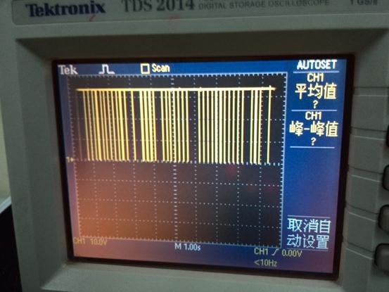
心得体会:
通过这些实验的设计与操作,我们深深体会到DSP的理论知识与实践相结合的重要性。在老师的指导下,我们完成了DSP的所有实验,并学会了CCS 3.1版软件,DSP仿真器,E300实验箱,DSP-54XP CPU板等的基本操作,掌握了外部中断的处理方法,键盘的基本编程方法、Liquid Screen 的基本编程方法、CUP定时器中断方式控制程序流程A/D转换模块的使用、PWM波的使用方法,同时非常感谢老师和同学们的帮助。
-
dsp实验报告
DSP实验课大作业实验报告题目在DSP上实现线性调频信号的脉冲压缩动目标显示和动目标检测一实验目的1了解线性调频信号的脉冲压缩动目…
-
dsp实验报告心得体会
TMS320F2812xDSP原理及应用技术实验心得体会1.设置环境时分为软件设置和硬件设置,根据实验的需要设置,这次实验只是软件…
-
dsp实验报告
西南科技大学城市学院-----课程设计报告题目:基于DSP2407的数字电压表系别:机电工程系专业:电信班级:1101指导教师:实…
-
dsp课程设计实验报告总结
DSP课程设计总结(20##-20##学年第2学期)题目:专业班级:电子1103学生姓名:学号:指导教师:设计成绩:20##年6月…
-
dsp的实验报告和ccs的基本操作
实验报告课程名称DSP原理与应用实验名称CCS的使用专业通信工程班级学号姓名指导教师20xx年3月25日实验一CCS的使用实验名称…
-
dsp实验报告心得体会
TMS320F2812xDSP原理及应用技术实验心得体会1.设置环境时分为软件设置和硬件设置,根据实验的需要设置,这次实验只是软件…
-
dsp课程设计实验报告总结
DSP课程设计总结(20##-20##学年第2学期)题目:专业班级:电子1103学生姓名:学号:指导教师:设计成绩:20##年6月…
-
dsp实验报告
DSP实验课大作业实验报告题目在DSP上实现线性调频信号的脉冲压缩动目标显示和动目标检测一实验目的1了解线性调频信号的脉冲压缩动目…
- dsp实验报告
- dsp实验报告
-
dsp实验报告
FIR数字滤波器的设计目录1前言22数字滤波器及MATLAB语言概述221数字滤波器的定义和分类322常用滤波器的性能指标423M…